Whenever you get a new board and it doesn’t work as you would expect, it can be a maddening experience. Some designers will break out their multimeters and start probing voltage measurements around the board while others will start looking at footprints and part numbers in their design documents to see if their manufacturer made a mistake during production. No matter what your initial reaction is in this type of situation, almost every designer can accept that circuit board troubleshooting is a time-consuming process.
The toughest part of troubleshooting circuit boards during bring-up and testing is the need to trace interconnections throughout your design. The ability to see your internal traces and track nets throughout the design is now much easier with some simple yet powerful augmented reality (AR) tools. If you have never developed a strategy for troubleshooting a circuit board, AR applications like Inspect AR can help ease the pain of circuit board troubleshooting and locating faults.
Where Are the Defects?
When troubleshooting circuit boards, there are several areas to check in the board, and how you approach these areas will inform your troubleshooting strategy. If a board is not functioning as you expect in your design, there are four areas you should check:
- Design defects: This can include any type of mistake that may have been made in the design data, which was subsequently reflected in the fabrication data. In some cases, apparent fabrication or assembly defects are really design defects and vice versa.
- Fabrication defects: Some fabrication defects are obvious and can be measured with probes. Others are tricky and you have to infer they’ve occurred by comparing measurements with your design data.
- Assembly defects: An assembly defect can range from a completely bridged component to tombstoning or fractured solder joints. When probing the board, you might be able to pinpoint specific areas of the design that should be investigated further for assembly defects.
- Component defects: These don’t occur often, but sometimes a component is simply defective, and this might cause the problems you observe during testing. In other cases, the wrong component was placed, either because an incorrect component was ordered or placed in the design data.
A comprehensive troubleshooting strategy will give you the opportunity to inspect multiple areas at once and, ideally, pinpoint defects to specific sections of the board. In some cases, you might narrow the problem to a specific component, net, or other feature on a circuit board and you can focus on that area to pinpoint the problem.
Troubleshooting Circuit Boards
Step One: Start Visually
If the board doesn’t work as designed on first power up, the first step is to do a visual inspection, ideally with a magnifying glass or microscope. Simple problems like soldered shorts between pins on components, tombstoned components, missing components (accidentally DNP’d), or footprint mismatches can usually be identified visually. If the component footprints and symbols are incorrect in your design data, there is a risk the pad/hole arrangement does not match the real component, and you might leave a short or open circuit after assembly. Some low-budget fabricators will produce boards that have obvious defects like this and may not do sufficient inspection or testing during assembly, possibly leaving you with a defective board.
Step Two: Move On to Measurements
If the board passes a visual inspection, you can move on to taking measurements. You’ll typically need to break out a multimeter to check that you’re getting power, opens, and shorts where you expect them. If you’re not seeing power/opens/shorts on expected nets, you might have a faulty component, a fabrication defect, or an assembly defect. Electrical testing during fabrication is intended to locate these problems, but these tests may register as passing if there is an error in your design files. You’ll need to take a series of measurements to distinguish a fab/assembly defect from a faulty component.
Step Three: Test Components
During troubleshooting, removing a component from the board and testing it should only be done as a last resort. For very small components (e.g., 0402 or smaller) or parts with dense pins, you might find it difficult to re-solder the component back onto the board should they be found to function correctly. It’s even possible that a very slightly lifted yet working component produces an open circuit that appears to be a faulty component. This is the type of thing you might miss in a visual inspection, but it can still cause the board to fail testing.
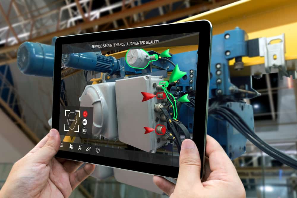
Troubleshooting a Circuit Board Is Easier With Inspect AR’s Augmented Reality Tools
After doing a visual inspection, designers will need to open up the design files on their computer and try to trace net connections on screen while they take measurements on the physical board. This is a major time waster and it opens up the possibility of measurement errors. On a dense board, it’s easy to mistake components, pads, and vias for those with different net connections, leading to measurement mismatches during inspection.
The power of augmented reality tools like InspectAR is the ability to see your design data overlaid on your PCB layout during testing and troubleshooting. With this perspective, you can see the connections that were placed in the design data and deduce the measurement you would expect to see on your meter. When your measurement doesn’t match your expectation, you can start looking further into the problem area.
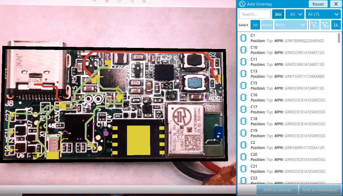
Using InspectAR to view nets on a Maxim Integrated reference design. Note that nets and component information are overlaid on the design
At this point, your goal is to determine whether the problem you have identified is caused by a faulty component, a fabrication defect, or an assembly defect. Inspect AR enables you to see the problem area and all associated traces/components as soon as they are identified. In addition, you can see MPNs for parts on the problem interconnect, access footprints from the datasheet, and compare these with your design data in a single window.
When you need to find electrical data and ECAD models for different types of PCBs that are verified by component manufacturers, try using the electronics search engine features in Ultra Librarian. Additionally, troubleshooting circuit boards is much easier when you can instantly see your design data overlaid on your prototype with the augmented reality features in InspectAR. Both platforms are compatible with popular ECAD applications and will help you streamline your verification process.
Working with Ultra Librarian sets up your team for success to ensure streamlined and error-free design, production, and sourcing. Register today for free.


 compared to a traditional USB-A cord (right).")