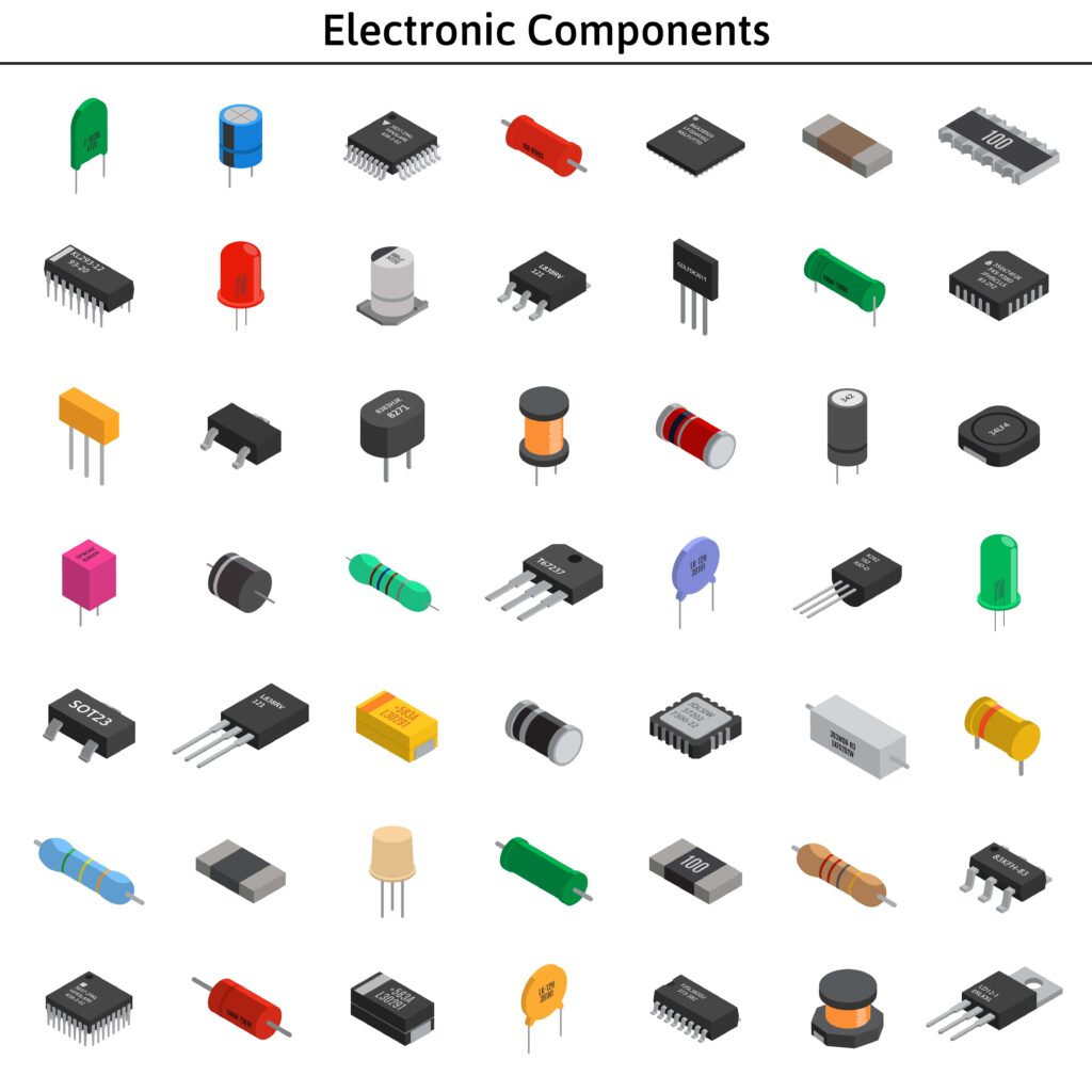
Electronic components come in all shapes and sizes.
When it comes to designing circuit boards, size does matter! Electronic components come in all shapes and sizes. The same is true for PCBS. Nevertheless, there are limitations.
The boundaries to which your imagination can go as a PCB designer or engineer are only limited by your CM’s equipment and capabilities. Regardless, whether you are designing rigid, flex, or rigid-flex boards, there are standards that your CM must adhere to. To aid your CM and create the most efficient PCB development process, it to most helpful to know and utilize standards as found an a SMT components size chart.
SMT Components Size Chart
SMT parts may be active or passive devices and packaged as discrete components or integrated circuits (ICs). For discrete SMDs, the following chart lists the different component sizes.
Sizes for surface mount ICs vary a great deal. Type and number of internal components are significant determining factors. Multi-component ICs or MCOs that contain two, three, four, or more discrete parts are very common, and often preferred as they simplify board layout and routing. However, there are standard IC package types and manufacturers that utilize them must comply with industry standards; such as IPC-7351 that provides guidelines for SMT component design and requirements for PCB footprints.
Many components are available in most, if not all, of the dimensions shown in the SMT components size chart, above. Therefore, you typically have several options for your design. To make the best use of this information for your design, it is important to understand how SMD size impacts the board development process.
How Component Size Impacts PCB Development
Undoubtedly, component selections are among the most important decisions for designing PCBAs. However, the impact of those choices permeates throughout all three phases of PCBA development: design⇒build⇒test (DBT).
PCB Design Considerations
In many cases, whether to opt for surface mount components vs through hole elements is a major PCB design consideration. When making this decision, size can be the determining factor. Generally, surface mount devices (SMDs) are smaller enabling more compact designs and products due to their greater PCB component density. However, there are spacing guidelines and restrictions on clearance and creepage, board edge clearance, space for depanelization, and other considerations that can impact your SMT component size selections.
PCB Manufacturing Considerations
From a manufacturing perspective, surface mount components allow for more automation and less soldering errors. Bulk reel packaging and pick and place machines virtually eliminate the need for human intervention for surface mount technology (SMT) PCB assembly. Although, pick and place machines for through hole placement are available, many parts require manual placement due to their shape and/or size. Additionally, reflow soldering results in less rework to correct errors like solder bridges or cold solder joints, which are more likely with the more traditional wave soldering.
PCB Testing Considerations
The final stage before a circuit board can be released from development and go into production is testing. PCB testing is typically performed by test engineers after manufacturing. However, some inspections and tests are routine steps in both fabrication and assembly. For SMT components, testing, especially functional, can be challenging due to their size and corresponding component density on the board. If in-circuit tests (ICTs); such as flying probe–that require a dedicated apparatus be assembled–are employed, additional board real estate must often be allotted for special testpoints.
Incorporating SMD Size Into Your Design
Although, the use of electronic circuit boards is growing exponentially, the electronics product market is highly competitive. This places increased demand on PCB designers and engineers to not only create designs that meet or exceed performance objectives, but also to design for optimization of the PCBA development process. This includes incorporating design for manufacturing (DFM), design for assembly (DFA), design for testing (DFT) and other guidelines and best practices to aid your CM, test engineer and other ECAD/MCAD team members achieve the highest quality board as efficiently as possible. Understanding the importance of and effectively using SMT components size chart information, as listed below, can significantly aid this effort.
 Know what component sizes available for your component(s)
If you’re looking for CAD models for common components or design information on how to best use a SMT components size chart for your design, Ultra Librarian helps by compiling all your sourcing and CAD information in one place.
Working with Ultra Librarian sets up your team for success to ensure streamlined and error-free design, production, and sourcing. Register today for free.