
Most HDI (high density interconnect) designers and many high speed designers are familiar with BGA (ball grid array) components, which provide a way to connect dense, high pin-count components to a PCB. These components function as a standard flip-chip BGA, but without solder balls for surface-mounting. LGA (land grid array) packages are designed to fit either into a specific LGA socket, or they can be soldered using standard SMD assembly techniques.
On the design side, you need access to accurate LGA package footprints when placing these components in a PCB layout. What information needs to be included in an LGA, and what is the difference between the socket and the actual component package? When you need to find LGA package footprints for your components, an electronics search engine can help you find the footprints you need for your LGA, as well as for any other components you need.
BGA vs. LGA Package Footprints
Since most designers are familiar with BGA footprints and mounting, they deserve a comparison with LGA components. A BGA component includes solder balls on the bottom of the component, and the solder balls mount directly to pads on the PCB. The designer needs to use an escape routing on the surface layer or through interior layers to reach the BGA pads. This mounting style is popular for many high pin-count components, such as FPGAs or baseband chips in mobile products.
An LGA attaches to a socket, and the socket attaches directly to the board using through-hole mounting or SMD mounting. The LGA socket or the component itself may contain some smaller passives to support the component functions. This means, when designing a PCB with an LGA, LGA package footprints need to include pad or hole locations, which define where traces will be routed to send signals to components. The actual IC then mounts to the LGA socket and snaps in place with a mounting bracket. This is the standard method for placing CPUs in new computers.
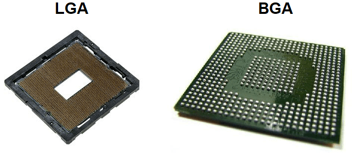
If you look at BGA and LGA package footprints, they look very similar, but there are some key differences. Both types of components contain arrangements of pads to match the pitch and layouts required on the PCB. For a BGA, the only other required information is a courtyard outline and possibly a silkscreen outline. Note that you should include an indicator in your PCB footprint for pin 1 on the component.
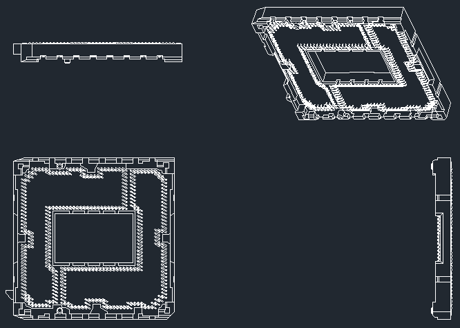
For an LGA, the component is more complicated and contains some mechanical mounting brackets. The LGA also contains an arrangement of pads or holes for mounting, but it also contains some mechanical brackets to attach the LGA component to the socket. These mechanicals need to be defined in the PCB footprint on a mechanical layer. This is quite important for ensuring you maintain minimum clearances from nearby components.
What to Include in Your LGA Footprint
The pad arrangement for each type of component can be easily created from a datasheet, but a 3D model for an LGA is more complicated than for a BGA. An IC with BGA mounting will only need, at minimum, a simple black box to represent the component. In contrast, a 3D model for an LGA requires the socket, backplate, and top bracket to fully represent the component.
If you’re not a mechanical designer, you can define the outer limits for LGA footprint packages by extending the component courtyard to match the socket and bracket outline. You can also design simple mechanicals for the socket and bracket that match the outer edges of the component, which will define a simple outline for the LGA socket and bracket. Be sure to check your datasheets when creating your own component footprints and models.
A better way to find all the component data you need, including LGA footprint packages, is to use an electronic parts search engine service. You can save yourself time when creating footprints for your components and you’ll know your footprints and 3D models will be correct. DXF, STP, and IGS files can be easily found with the right service and these models can be used to define the mechanical portion of your LGA package footprints.
Use a Search Engine for LGA Footprints
Instead of staring at a datasheet and drawing outlines in a CAD application, you should try using a comprehensive parts search engine to find your component data. You’ll be able to quickly find schematic symbols, PCB footprints, 3D models, specifications, and sourcing information for your components. This helps you qualify new components before you start a new design, and you can quickly bring component data directly into your ECAD software.
This lets you see component specs directly in your search results, and you can quickly narrow down to some candidate components before you start combing through datasheets. You can also take advantage of integrated search features in your CAD applications to quickly fund verified models and datasheets for your components.
Next time you need LGA package footprints for a new design, try finding the components you need from a parts search service like Ultra Librarian. You’ll have access to a range of 2D and 3D LGA package models from major manufacturers, and you’ll see real-time sourcing information from worldwide distributors. You can then import your data into popular ECAD applications and use your new components in your designs.
Footprint and 3D electronic component model creation takes dedicated resources and time, but Ultra Librarian helps streamline these processes. Working with Ultra Librarian will set up your team for success and ensure your finished product matches your design. Register today for free!


")