
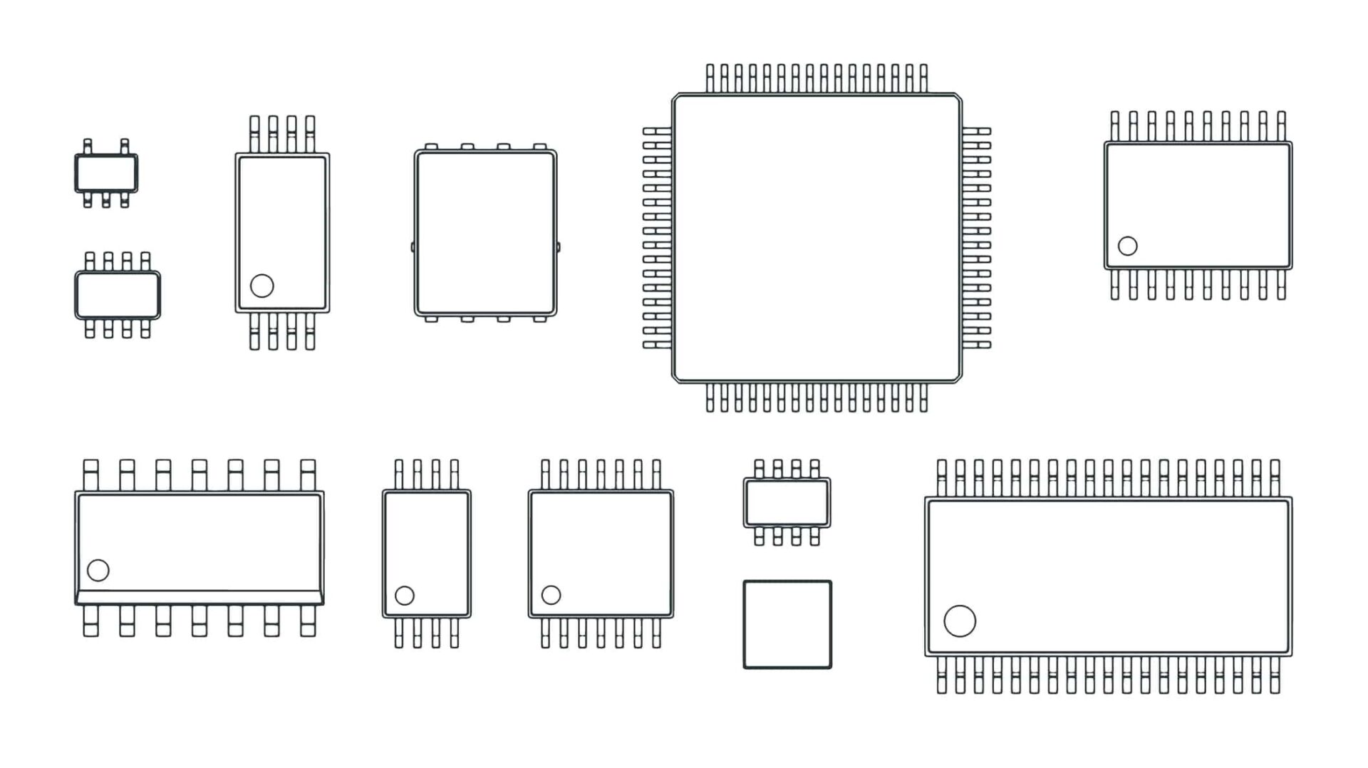
Examples of common IC packaging designs
Integrated circuits, or ICs, come in all shapes and sizes. This variety is necessary to meet the dimensionality constraints that vary from application to application. Silicon (Si) is the most utilized semiconductor material for manufacturing ICs. Its natural abundance, ease of processing, and low costs are some of the advantages contributing to its popularity.
However, as frequency and power requirements for ICs are continually pushed, inherent physical limitations with Si have resulted in the increased research into and development of other III-V semiconductor-based chips, such as gallium nitride (GaN). At Texas Instruments, the properties of GaN technology are being maximized through advanced IC packaging design techniques to help push performance capabilities for high-power density applications like hyper-scale data centers and personal electronics.
The Impact of Power Density on PCB Design and Operation
Aside from minimizing noise, effectively managing power is the most critical problem facing PCBA designers in power systems or high-power-density applications. Therefore, before discussing the utilization of IC packaging design, it is informative to understand why power density, defined below, is essential.
| Definition:
Power density quantifies how much power can be or is processed within or through a given physical space. |
For IC packaging design, high power density, or the ability to maximize power in a given space, is an essential parameter, as managing heat can be a major challenge.
Similarly, thermal management is often a critical aspect of ECAD/MCAD, as excess heat can cause erroneous performance or even damage the board and its elements.
Techniques for Improving Power Management
For high-power electronics, excess power losses—which occur due to heat generated in the semiconductors—typically cause thermal issues and contingencies. Therefore, many of the design techniques that engineers employ, including those listed below, focus on increasing the current flow area.
Methods for Thermal Management
- Heat sinks to dissipate heat from the top of parts
- Thermal vias to dissipate heat from the bottom of parts
- Spacing high-power components apart on the board
- Higher board thicknesses
- Wider traces and thicker copper
The design techniques above are effective; however, they all have limitations. For example, traces and vias are limited by spacing requirements, which is a major problem for small boards or tight installations. Fortunately, IC manufacturers have been working to address this issue.
Many companies now produce components designed to be more resilient to thermal issues. At TI, pursuing advanced power process nodes continues to improve component power performance and efficiency.
Additionally, TI has developed advanced IC packaging designs that help improve PCB power density.
IC Packaging Design Innovations to Optimize Power Management
Optimizing power management effectively means maximizing power density at the upper limits of performance for high-power applications. Process technologies and design techniques are essential and should be instituted. However, improving IC packaging design is an often overlooked area for optimizing power density.
The figure below illustrates an example of TI’s innovations in this area.
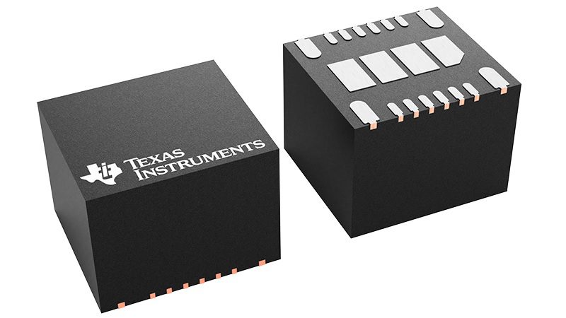
Power density optimized IC package design by TI
The figure above shows the TI TLVM13660 power module in an enhanced HotRod™ package. This package leverages the quad-flat no lead (QFN) design that minimizes the required board surface area and allows for a smaller overall board size. However, perimeter pin placement provides flexibility in design. Fan out, and vias can be implemented to reduce or eliminate surface heat and hot spots and increase thermal dissipation.
Additionally, enlarged die attach pads (DAPs) are implemented to facilitate faster heat transfer.
These IC packaging innovations increase power density and improve thermal management, pushing the limits on performance capabilities for advanced technology development.
Suppose you’re looking for CAD models for common components or innovative solutions for advanced PCB development like IC packaging design to increase power density capabilities. In that case, Ultra Librarian helps by compiling all your sourcing and CAD information in one place.
Working with Ultra Librarian sets up your team for success to ensure streamlined and error-free design, production, and sourcing. Register today for free.


")


")