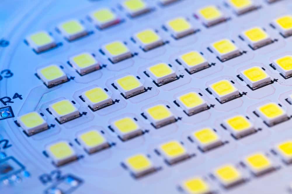
The SMD LED footprint needs to be designed to align precisely with the component for automated pick-and-place machines
An SMD LED (surface-mount device, light-emitting diode) is characterized by its compact size, surface-mount design, and flat package. Typically, it consists of two or more metalized pads on a printed circuit board (PCB) surface, where the LED is soldered. The SMD LED footprint includes solder pads or solder resist areas for electrical connection and alignment features to ensure precise placement during PCB assembly.
The footprint size varies depending on the SMD LED package type, with common variants including 0402, 0603, 0805, and 1206, indicating dimensions in metric units. These footprints are designed to accommodate automated pick-and-place machines, enabling efficient assembly processes in high-volume manufacturing environments. The SMD LED footprint offers miniaturization, assembly efficiency, and thermal management advantages, making it well-suited for a wide range of applications requiring compact and reliable lighting solutions.
SMD LED Footprint vs THT LED Footprint
An alternative to an SMD LED is a through-hole technology (THT) LED. They differ in several key characteristics. SMD LEDs are compact and suitable for automated assembly processes, offering miniaturization and assembly efficiency benefits. In contrast, THT LEDs have a larger footprint, cylindrical or dome package, and THT mounting, providing mechanical stability and better heat dissipation capabilities. They are often preferred in applications where mechanical robustness and durability are critical, though they require more space on the PCB and may involve additional manual soldering steps. The table below compares SMD LED and THT LED in terms of their main characteristics.
|
SMD LED vs THT LED: Characteristics |
||
|
Characteristic |
SMD LED |
THT LED |
|
Size |
Smaller footprint |
Larger footprint |
|
Mounting |
Surface mounted |
Through-hole mounted |
|
Package Type |
Flat package |
Cylindrical or dome package |
|
Assembly |
Automated assembly preferred |
Manual or automated assembly |
|
Heat Dissipation |
Typically lower power, less heat generated |
Can handle higher power, better heat dissipation |
|
Placement Flexibility |
Can be placed closer together, allowing for higher density |
Requires more space on PCB due to larger footprint and leads |
|
Assembly Efficiency |
Faster assembly process because of pick-and-place machinery |
Requires additional steps for manual soldering |
|
Mechanical Stability |
More susceptible to mechanical stress and damage due to surface mounting |
More stable due to through-hole mounting |
|
Component Height |
Lower profile, suitable for applications with limited vertical space |
Higher profile, may not be suitable for applications with height constraints |
|
Structure around LED |
Typically includes solder pads or solder resist for electrical connection |
Includes leads for through-hole soldering, may also have additional structural support |
Overall, SMD LEDs excel in compactness and efficiency, while THT LEDs offer reliability and mechanical stability, catering to diverse requirements in various lighting and electronics applications.
SMD LED Structure

PCB with SMD LED modules
The SMD LED structure comprises several components designed to ensure proper functionality and integration into a PCB. At its core, the SMD LED features a semiconductor chip that emits light when electrically stimulated. Here are the structural components of an SMD LED:
- Flat package encapsulating the LED semiconductor chip
- Metalized pads or terminals on the bottom surface for soldering onto the PCB
- Materials like epoxy or silicone for environmental protection and mechanical stability
- Alignment features such as polarity markers or chamfered edges for accurate placement during assembly
Overall, the structure of an SMD LED is designed to provide protection, electrical connectivity, and alignment, ensuring reliable performance within various electronic devices and lighting applications.
If you’re looking for CAD models for common components or SMD LED footprint information, Ultra Librarian helps by compiling all your sourcing and CAD information in one place.
Working with Ultra Librarian sets up your team for success to ensure streamlined and error-free design, production, and sourcing. Register today for free.


