To optimize signal integrity, PCB antenna design and RF layout guidelines must be followed
When developing RF communication systems, a good deal of attention is paid to transmit and received power, signal attenuation and path loss, interference and other channel parameters. Although, these specifications are important, undervaluing the onboard design will result in a low quality, unreliable system. In fact, an optimal communication system depends on the understanding and following of good antenna design and RF layout guidelines.
Antenna Design and RF Layout Guidelines To Know
Just as for power and digital signals, there are a number of common connectors for attaching RF signal antennas to PCBAs. Additionally, antennas may be fabricated onto the circuit board. When designing boards with these PCB antennas, it is important to know and follow layout guidelines, as listed below.
The list above is not exhaustive, but does include the most important antenna and RF layout guidelines to incorporate into your PCBA design. The criticality of following these can be best appreciated by looking at the challenges for PCB antenna design.
PCB Antenna Design Challenges
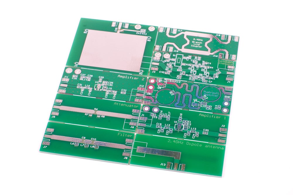
Common PCB antenna types include the following: loop, monopol, dipole, microstrip, slot, patch, and planar inverted-F antenna (PIFA). As this list indicates, PCB antennas come in various shapes and sizes. Each is formed by isolating flat conductive areas on the surface of the board. And they present common challenges for your board design.
 Impedance Matching
As shown above, there are significant challenges when design circuit boards with antennas. The best way to address these issues is to follow good antenna design and RF layout guidelines. The degree to which this is done dictates the quality of your design and how well your PCB antenna circuit will perform.
How to Optimize Your PCB Antenna and RF Design
There are options for designing PCB antennas. Most importantly is choosing among the various antenna types, which have different size and shape requirements. For example, you may opt for a separate antenna PCB that can be connected to a RF circuitry module, as opposed to a custom board design. In either case, the importance of knowing and implementing PCB antenna design and RF layout guidelines cannot be overstated.
Incorporation of antenna design guidelines; however, can vary. Yet, prioritizing the following considerations can help you achieve the most efficient implementation and optimize your PCB antenna design process.
PCB Antenna Design and RF Layout Optimization Considerations
- Choose your antenna type based on dimension constraints.
- Use simulation to validate antenna operation and determine electromagnetic effects.
- Select components based on antenna specifications.
- Source components from a reliable source.
- Augment your PCB layout best practices with good antenna design and RF layout guidelines.
If you’re looking for CAD models for common components or PCB best practices like antenna design and RF layout guidelines, Ultra Librarian helps by compiling all your sourcing and CAD information in one place.
Working with Ultra Librarian sets up your team for success to ensure streamlined and error-free design, production, and sourcing. Register today for free.