
Applications for the TCK42xG series MOSFET driver
December 23, 1947, was a day that changed the world. Although most people were unaware of its significance, this is when the transistor made its first public appearance. This semiconductor has continually evolved while also changing almost every facet of our lives by controlling and driving the electronics and technology we use and rely upon.
Today, metal-oxide-semiconductor field-effect transistors (MOSFETs) – the most implemented transistor type – can be found in virtually all products, including electronics and circuit boards. This includes spacecraft, airplanes, automobiles, mobile phones, and wearables. However, the performance of these critical components depends upon power management as provided by the TCK42G series of MOSFET driver ICs from Toshiba.
Features and Applications of the TCK42xG Driver
The TCK42xG is a series of six MOSFET gate driver ICs for power line application. The drivers are designed to be utilized at the following voltage levels. TCK42xG series is an Over Voltage Protection Gate Driver IC for External N-channel MOSFET. This product supports MOSFET operating in a wide voltage line from 2.7 V to 28 V with various Over Voltage Lock Out lineups. And this features low standby current, less than 1 µA, built in charge pump circuit and MOSFET gate-source protection circuit. Package is very small and thin WCSP6G (1.2 mm x 0.8 mm (typ.), t: 0.35 mm (max)). Thus this is suitable for mobile, wearable systems and power management circuits such as load switch applications.
The drivers are intended for use in N-channel common drain and single high side MOSFET circuit configurations and have the following features.
TCK42xG Series Gate Driver Features
- Gate driver for N-channel Common Drain MOSFET
- Gate driver for N-channel Single High side MOSFET
- High maximum input voltage: VIN max = 40 V
- Wide input voltage operation: VIN = 2.7 to 28 V
- Gate-Source protection circuit
- Over Voltage Lock Out : VIN_OVLO = 6.31 V, 10.83 V, 14.29 V, 23.26 V and 27.73 V typ
- Under Voltage Lock Out : VIN_UVLO = 2.0 V typ
- Built in Charge pump circuit: Gate source voltage VGS = 5.6 V and 10 V typ
- Low standby current : IQ(OFF) = 0.9 µA max at VIN = 12 V (Except TCK424G, TCK425G)
These features enable the TCK42xG to be implemented in many situations to provide power management; however, primary applications include wearables, mobile devices, and IoT systems.
TCK42xG Series Specifications
Absolute ratings for safe operation are listed in the table below.
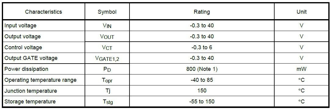
Absolute ratings for the TCK42xG
As the TCK42xG series includes a wide range of voltage levels, there is a range of DC characteristics. These are shown below.
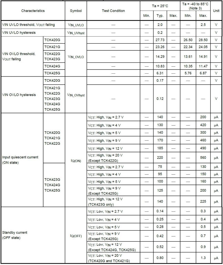
DC Characteristics for the TCK42xG
The following table details the range of gate drive voltage values.
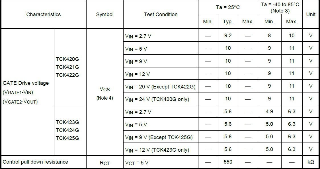
Gate drive voltage options for TCK42xG drivers
MOSFET Driver Operation
VGATE1 pin is connected to Gate of the VIN side MOSFET. The VGATE2 pin is connected to Gate of the VOUT side MOSFET. VOUT pin is connected to Source of VOUT side MOSFET. When the gate driver IC turns off state, VGATE1 terminal voltage is close to VIN voltage dropped by parasitic diode forward voltage. This circuit works to protect over voltage for VIN side MOSFET Gate-Source terminal. VOUT terminal works to protect VOUT side MOSFET from the same circuit as shown in the typical application diagram below.
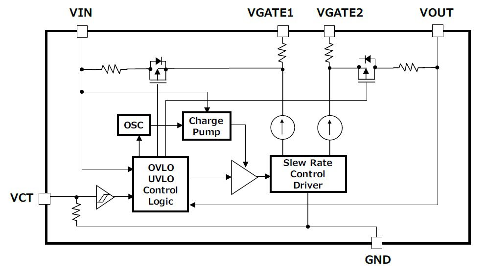
Typical application diagram of the TCK42xG block diagram
The component can operate in two power modes (ON and OFF), which VCT controls. However, one or two external MOSFETs can be controlled in ON mode. This is shown in the table below, along with descriptions for all six pin connections.
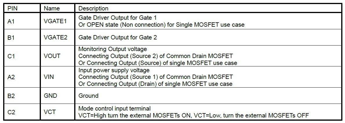
TCK42xG pin descriptions
Circuit layout examples of these two operation modes are shown below.
Application Examples
The most typical circuit design with the TCK42xG drivers is a common drain configuration, as illustrated below.
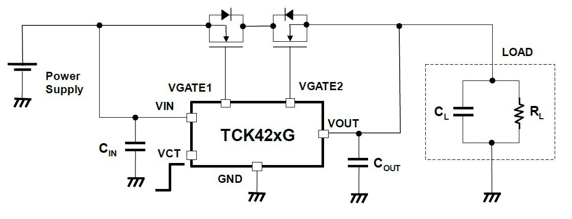
Typical TCK42xG design
NOTE: It is highly recommended that input and output capacitors be included to aid in stabilizing power supply operation. These components should be placed as close to the input and output pins as possible. Single MOSFET operation is an option, and the preferred circuit design leaves VGATE1 open with VGATE2 supplying the gate voltage for the external MOSFET.
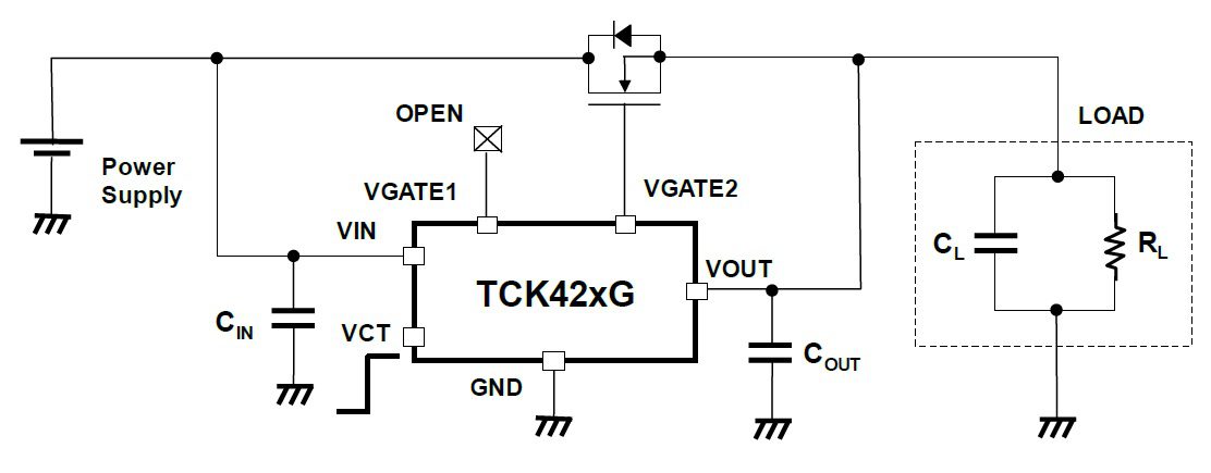
Single MOSFET design with TCK42xG gate driver
When designing circuits with these MOSFET drivers, you should consult and follow the guidelines in the TCK42xG series datasheet.
Optimal Design with the TCK42xG Gate Driver
Toshiba’s series of MOSFET gate drivers are intended to provide you with a wide range of options for power management in commercial applications like wearables, mobile devices, and IoT systems.
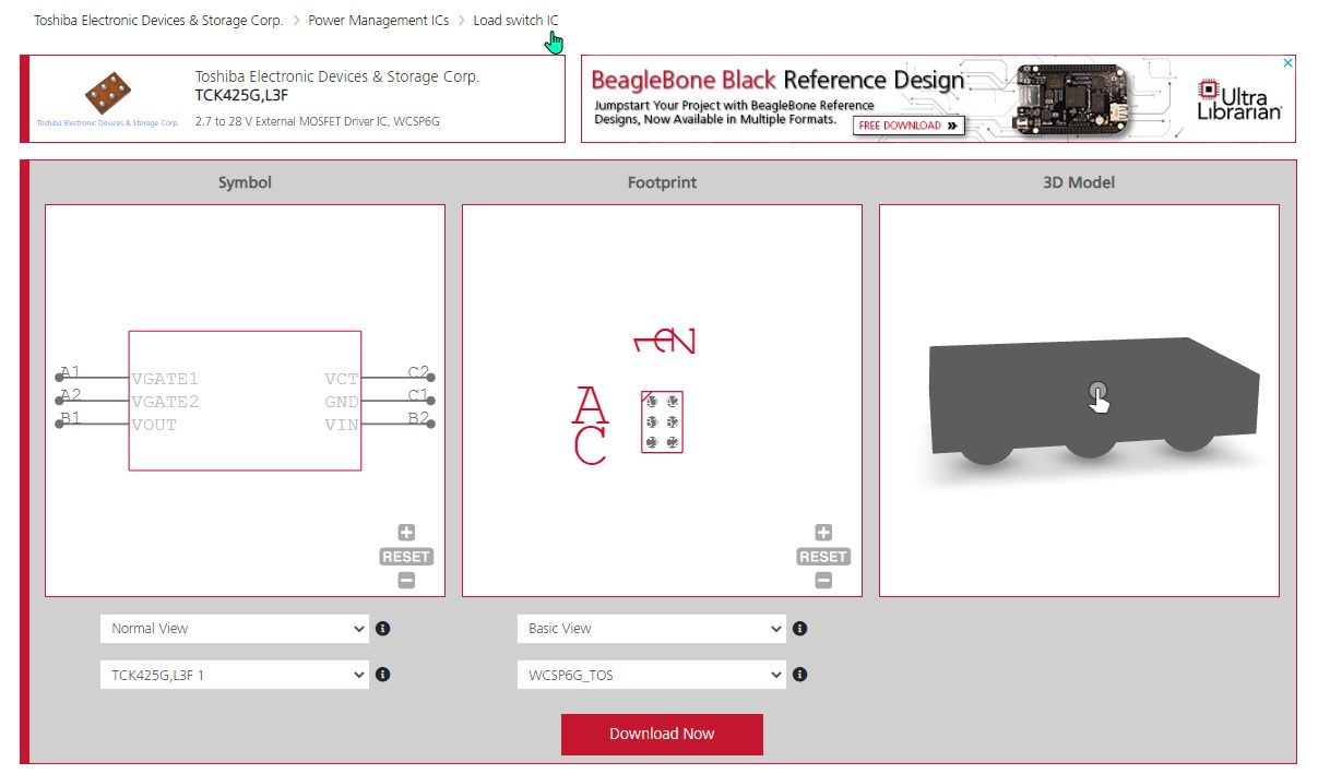
CAD data for TCK425G gate driver
In addition to using the datasheet and other reference design information for the TCK42xG series from Toshiba, it is also essential to make sure that you create your PCB layout with verified CAD data, as shown in the figure above, from a proven component data source. This will ensure the manufacturability of your board and enable you to work with your CM to make the development process for your TCK42xG series circuit design as efficient as possible. You can realize a superior solution for power switch with small size, low On-resistance and additional protection feature with any MOSFET you can choose.
If you’re looking for CAD models for common components or power management solutions to protect and improve the reliability of your MOSFET-based applications like the TCK42xG series of gate drivers, Ultra Librarian helps by compiling all your sourcing and CAD information in one place. Working with Ultra Librarian sets up your team for success to ensure streamlined and error-free design, production, and sourcing. Register today for free.


")