When a designer needs to create a component for a PCB board, they have many places where they can gather data – manufacturer websites, distributors, aggregators, or even crowd-sourced resources. However, the gold standard for information to build components is the manufacturer datasheet. This document provides all the information needed to build a component – PCB land pattern, schematic symbol pin-out, tolerances, ratings, electrical applications, and ordering information. Although there is a wealth of information included in datasheets, you only need a few key pieces of information to build your part. It can be difficult to sift through all of the information provided to determine exactly what you need to create a component. The Ultra Librarian team has built many components (14 million and growing) and has learned a few tricks to finding the information that you need in a datasheet in order to create library components.
Ordering Information
Some manufacturers provide a datasheet for each individual part number, but the majority of manufacturers provide a datasheet for a “family” of similar parts. The “ordering information” section of a datasheet will show you all of the individual part numbers associated with the particular family. This will often include the pin count and package information so you can be sure to have the right part number associated with the component you are creating. This section is typically displayed on either the first 1-2 pages of the datasheet or at the very end. It is a quick way to reference all of the part numbers provided in a certain part family as well as a little information about the component. It also will help you give the component the correct name.
‘Key’ Ordering Information Table. Source: Xilinx
If there are a large number of parts associated with a certain family, you may be given a ‘key’ to decode the individual part numbers. You would not want to name a component by the family name, as that does not provide enough detail for the specific part used. Instead, you will want to use the individual part number so you can be specific (for example: instead of naming a 16-pin TQFN Maxim component MAX16025 [family name], you would want to name the part MAX16025TE+ to denote the specific package & pin layout you are using).
Symbol Information
In order to create a symbol for your component, you will need to enter pin information. For larger pin parts (such as ball-grids or high-pin count IC’s), this can be the most painful part of component creation. Unfortunately, this information often needs to be entered by hand. Some manufacturers will provide IBIS or CSV files with symbol information, but this is rare. Most of the time, you will need to enter the information yourself – which can be quite challenging and time consuming.
Symbol information is typically found towards the beginning of the datasheet, however, each manufacturer differs in how they organize their datasheet. If a datasheet is particularly long, consult the table of contents and scan for sections like “Pinouts”, “Pin Information”, “Pin Layout”.
A 900 pin Xilinx Ball-Grind Pinout – quite a challenge! Source: Xilinx
You will typically see both a graphical representation of the component with pin names, as well as a table that includes pin name, pin number, and pin function, as well as any alternate functions that the pin may have (most common on programmable IC’s).
Graphical representation of pinout. Source: Silicon Laboratories
Pinout table, with pin names and alternate functions shown. Source: Silicon Laboratories
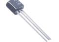
Additionally, for discrete components, there is usually a picture of what the symbol should look like graphically. For larger components and IC’s, a box symbol is fine. However, with smaller components, designers typically want to match the look (graphics) of their symbol to the graphic shown on the datasheet (which is usually an industry standard).
Graphic representation of symbol in the middle. Source: ON Semiconductor
Symbol information is typically found towards the beginning of the datasheet, however, each manufacturer differs in how they organize their datasheet. If a datasheet is particularly long, consult the table of contents, scanning for sections like “Pinouts”, “Pin Information”, “Pin Layout”.
Footprint and land pattern information is typically found towards the end of a datasheet. One datasheet can contain several packages, so it is always important to confirm that the footprint you are trying to build is the correct variant. The mechanical data includes information about the physical size of the component – height, width, row pitch, etc.
Mechanical Information. Source: Texas Instruments
The land pattern, if included, will provide specific information regarding the pads of the footprint. If the manufacturer has specific land pattern information for a footprint, it will often be included close to the mechanical information. As the creator of the footprint, you have the choice to follow the manufacturer’s recommended land pattern or follow another industry standard, such as the IPC.
Land pattern data. Source: Analog Devices (formerly Linear Technology)
Putting it all Together
Once you have gathered all of this information, you are ready to create your component. The datasheet has given you the information you need to:
- Specify the appropriate name for the part
- Create your logical symbol using pin tables and diagrams
- Create the physical footprint using mechanical dimensions
- You have found the appropriate name, entered the symbol information (creating a graphical representation)
- Once you have created the required logical symbol and land pattern in your desired CAD system you can now do things such as add attributes, or arrange your symbol in a more functional manner
The manufacturers datasheet is the ideal place to get all the info you need when creating components from scratch, however this can be time-consuming and error prone, especially if all of the entry is done manually. If you would rather avoid this work, why not create an account at UltraLibrarian.com and receive 15 free monthly ECAD downloads to the export of your choice? The Ultra Librarian team utilizes automated data collection and verification techniques, as well as manual reviews to ensure that the components we provide to the community are of the highest quality. See for yourself by creating an account at www.ultralibrarian.com today!