CD4017 Datasheet: Explained

Photo of CD4017B top and bottom

The CD4017B Counter from Texas Instruments

Many electronics projects eventually run into the same problem: you need to perform a series of operations in a specific order, one step at a time. Whether it’s advancing LEDs in a test fixture, stepping through stages of a diagnostic routine, or counting repeated events from a sensor, you need a simple and reliable way to convert a stream of clock pulses into clearly defined outputs.

This is exactly where the CD4017 shines. With ten decoded outputs and a simple clock-driven operation, it provides a dependable way to build event counters, step sequencers, and timing stages without the need for programmable logic. Its low part count, wide voltage range, and predictable behavior make it a staple in both classic and modern designs where straightforward sequencing matters.

Counter Circuits and Their Uses

Counters are fundamental building blocks in digital electronics, providing a simple way to track events, timing intervals, or sequence operations. At their core, counters use flip-flops that change state in response to a clock signal, producing a predictable progression of outputs, whether in binary, binary-coded decimal, Gray code, or a custom sequence. The total number of states a counter can represent depends on its modulus. Depending on the architecture, counters can update all flip-flops at once (synchronous) or allow state changes to ripple through one stage at a time (asynchronous). 

Common Counter Types 
Category Counter Type Description Use Case
Synchronous Counters Decade Counter Counts 0–9 (mod-10); outputs often BCD or one-hot decoded. All flip-flops share the same clock. Digital clocks, frequency division, numeric displays
Up/Down Counter Can increment or decrement based on a control signal; used for reversible position or event tracking. Motor/encoder position tracking, bidirectional event counting
Modulus Counter Custom mod-N counters designed to roll over at a specific count smaller than 2ⁿ. Timers, state machines, frequency dividers
Ring Counter A single ‘1’ bit circulates among flip-flops; a simple one-hot sequence generator. LED chasers, simple sequence generation
Johnson Counter A twisted ring counter with twice as many states; often used for sequencing and decode-friendly patterns. Pattern generation, timing signals, keypad scanning
Asynchronous Counters Ripple Counter Flip-flops toggle sequentially, each triggered by the previous stage’s output; simple but slower due to propagation delays. Low-speed counters, basic frequency dividers, simple timing circuits

CD4017 Counter Key Features

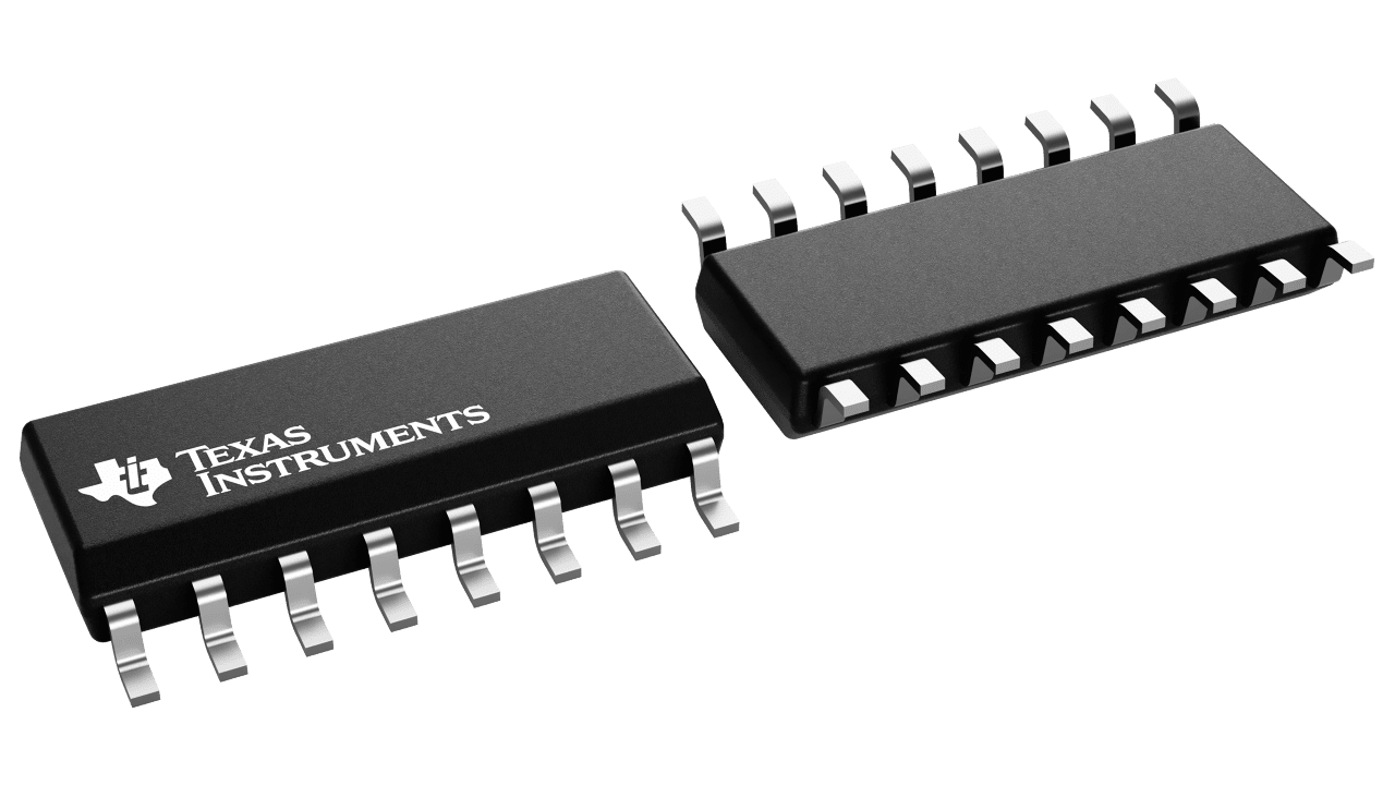
The CD4017 is a 5-stage Johnson decade counter designed for use across a range of digital logic systems. Its CMOS architecture provides very low power consumption (20 µA of supply current at 5 V (≈0.1 mW)), making it suitable for both battery-powered and mains-powered projects. With 10 fully decoded outputs, it can directly drive sequential indicators, such as LEDs, without requiring an external decoder. The CD4017 has a wide operating voltage range (3 V to 15 V) and is available in several common packages, including Plastic Dual In-Line Package (PDIP) for through-hole prototyping and Small Outline Integrated Circuit (SOIC) for compact surface-mount designs.

Key Features:

  • Supply Voltage: 3V–18V, compatible with low-power 3.3V/5V logic and higher-voltage industrial controls.
  • Output Characteristics: Can drive LEDs directly (with resistors) or interface with other CMOS/TTL logic gates.
  • Speed: Medium-speed operation, with typical max clock frequencies in the MHz range. Suitable for timing, sequencing, and control applications.
  • Cascadable Design: Carry Out (CO) pin enables easy linking of multiple CD4017 ICs for extended counting sequences.
  • Packages: PDIP, SOIC, SOJ, and TSSOP, allowing use in through-hole and surface-mount designs.

CD4017 Datasheet Pinout and Functions

The CD4017 is typically available in a 16-pin package, and its pins can be logically grouped into four main categories: the ten decoded outputs (Q0-Q9), the primary control inputs (Clock, Clock Enable, and Reset), the carry out signal for expansion or frequency division, and the power supply pins.

CD4017B Pinout and Functional Diagram.

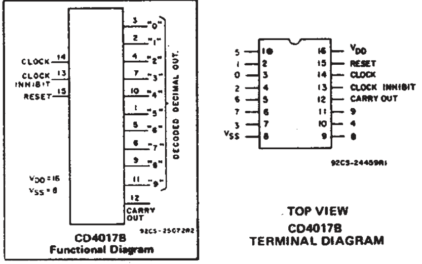
As you can see, the CD4017 is so fundamental that its pinout hasn’t needed to change for quite some time 


CD4017 Pin Functions
Pin # Name Type Description
1-7, 9-11 Q0 - Q9 Output Decoded Outputs: Ten individual outputs. As the clock pulses, each output (Q0, then Q1, Q2...) goes high in sequence for one full clock cycle. Only one output is high at any given time.
12 CO (Carry Out) Output Goes high during counts 0-4 and low during counts 5-9. This signal completes one full cycle for every ten input clock cycles, effectively acting as a divide-by-10 output. Used for cascading counters.
13 Clock Inhibit (CI) Input Clock Enable (Inhibit): When this pin is low, the counter advances on the rising edge of the clock. When high, the clock is ignored, and the counter pauses. Must be tied low for normal operation.
14 Clock Input Clock Input: The counter advances one step on each rising edge of the signal applied to this pin.
15 Reset (MR) Input Master Reset: Set High on this pin immediately resets the counter, forcing output Q0 high and all other outputs (Q1-Q9) low. Must be tied to ground for normal counting operation.
8 V SS Power Ground: The negative supply voltage reference (typically 0V).
16 V DD Power Positive Supply Voltage: The positive power supply for the IC (typically +3V to +18V).

CD4017 Absolute Maximum Ratings

When designing circuits with the CD4017, refer to the CD4017 datasheet to understand its maximum ratings. Staying within these specifications ensures reliable operation and prevents overstress to the device.

CD4017 Absolute Maximum Ratings
Parameter Value
DC Supply Voltage (V DD) -0.5V to +20V
Input Voltage Range -0.5V + DC Supply Voltage +0.5V
DC Input Current ±10mA
Power Dissipation (per package) 500mW
Power Dissipation (per output) 100mW
Operating Temperature Range -55°C to +125°C

CD4017 Practical Applications

The operation of the CD4017 is simple and straightforward. With connections to power, a clock source, and optional control pins, it can drive LEDs, relays, or other digital circuits without a microcontroller.

Basic Setup

  1. Power Supply: Connect VDD to positive voltage and GND to ground.
  2. Clock Input (CLK, Pin 14): Each rising edge of a pulse advances the counter by 1. Outputs Q0–Q9 go HIGH sequentially.
  3. Clock Enable (CI, Pin 13): HIGH disables counting; LOW enables normal operation.
  4. Reset (MR, Pin 15): HIGH resets the counter to Q0. LOW allows normal counting.
  5. Carry-Out (CO, Pin 12): Goes HIGH after 10 counts; can trigger another counter for cascading.

Running LEDs Applications

A common project using the CD4017 is an LED chaser, where each clock pulse from a timer or microcontroller advances the counter, turning on the next LED while turning off the previous one, creating a “running” light effect.

  • Use a 555 Timer in astable mode as a clock source.
  • Connect the 555 output to the CD4017’s CLK pin.
  • Attach LEDs to Q0–Q9 through resistors.
  • Each clock pulse lights the next LED in sequence.

Divide-by-N Applications

You can limit the counting to fewer than 10 steps by connecting Q(N+1) to the Reset pin. For example:

  • Count to 6: Connect Q6 → Reset
  • Count to 9: Connect Q10 → Reset

This allows flexible control for timers, LED sequences, and other digital circuits.

Cascading Counters

To extend counting beyond 10:

  • Connect the CO pin of the first CD4017 to the CLK pin of the next.
  • Keep Reset and Clock Enable pins LOW.

 This allows chaining multiple ICs for larger sequences, e.g., 0–99 counters.

When implemented correctly, the CD4017 delivers reliable, sequential counting and decoding for a wide range of digital logic applications, from LED chasers to frequency dividers.

If you’re looking for the CD4017 datasheet or CAD models, Ultra Librarian helps by compiling all your sourcing and CAD information in one place. The platform provides verified, ready-to-use footprints, schematic symbols, and 3D models compatible with all popular ECAD tools, along with sourcing information from global distributors.

Working with Ultra Librarian sets your team up for success, ensuring streamlined and error-free design, production, and sourcing. Register today for free.

UL-Icon.png

The Ultra Librarian Team

Ultra Librarian offers the world’s largest PCB CAD library, putting cutting-edge materials at your fingertips so you can build better products faster—all for free.

Join Our Newsletter

Subscribe to our newsletter to receive the latest news, and important updates

Name(Required)

Related Posts

If you’re looking for any of our component footprints or models, we have readily available and free options for you and your design team. Search our library for the solution you’ve been looking for.

IC Manufacturers

Working with us allows you to target the right audience for your component, provide content to nurture them along their design process, and analyze how your parts are being received and used.

How do manufacturers help shape the pcb design engineer’s journey?

Download now to discover how manufacturers support PCB design with data, tools, models and more.

Part Details

Explore all the models within this part family

Free Design Resources

Ultra Librarian is the worlds largest online – and always free – PCB CAD library. Build products better, faster, and more accurately with easy access to vendor-verified symbols, footprints, and 3D models. Register today to start searching the right components for your next design.

Recommended

PHP Code Snippets Powered By : XYZScripts.com