
Key Takeaways
- Exploring the types and uses of active components.
- Looking at active components in electronic circuits.
- PCB layout considerations for active electronic components.
Arguably, the most important electronic component ever invented is the transistor. Developed in the late fall of 1947, this semiconductor device has served as the catalyst for the foundation of multiple corporations, helped launch Silicon Valley, and revolutionized the electronics industry. Not surprisingly, the invention of transistors earned Bell Labs researchers—William Shockley, John Bardeen, and Walter Brattain—a Nobel Prize in 1956. Today, it is estimated that trillions of these components are functioning in electronic devices worldwide and billions more aboard systems in space.
The transistor is an example of an active electronic component. Active electronic components require an external power source for their operation, enabling them to manipulate an applied signal to achieve a desired output signal. The ability to manipulate signals allows active components to amplify inputs, which is one of their most common applications. Due to the widespread manufacturing of active electronic components, matching your design’s library model with the actual component in your bill of materials (BOM) can be challenging. However, correctly matching the model to the physical part is essential for the manufacturability of your board and efficient PCBA development.
Let’s look at common types and uses of active electronic components, how they impact your PCB layout, and the importance of getting the CAD library right.
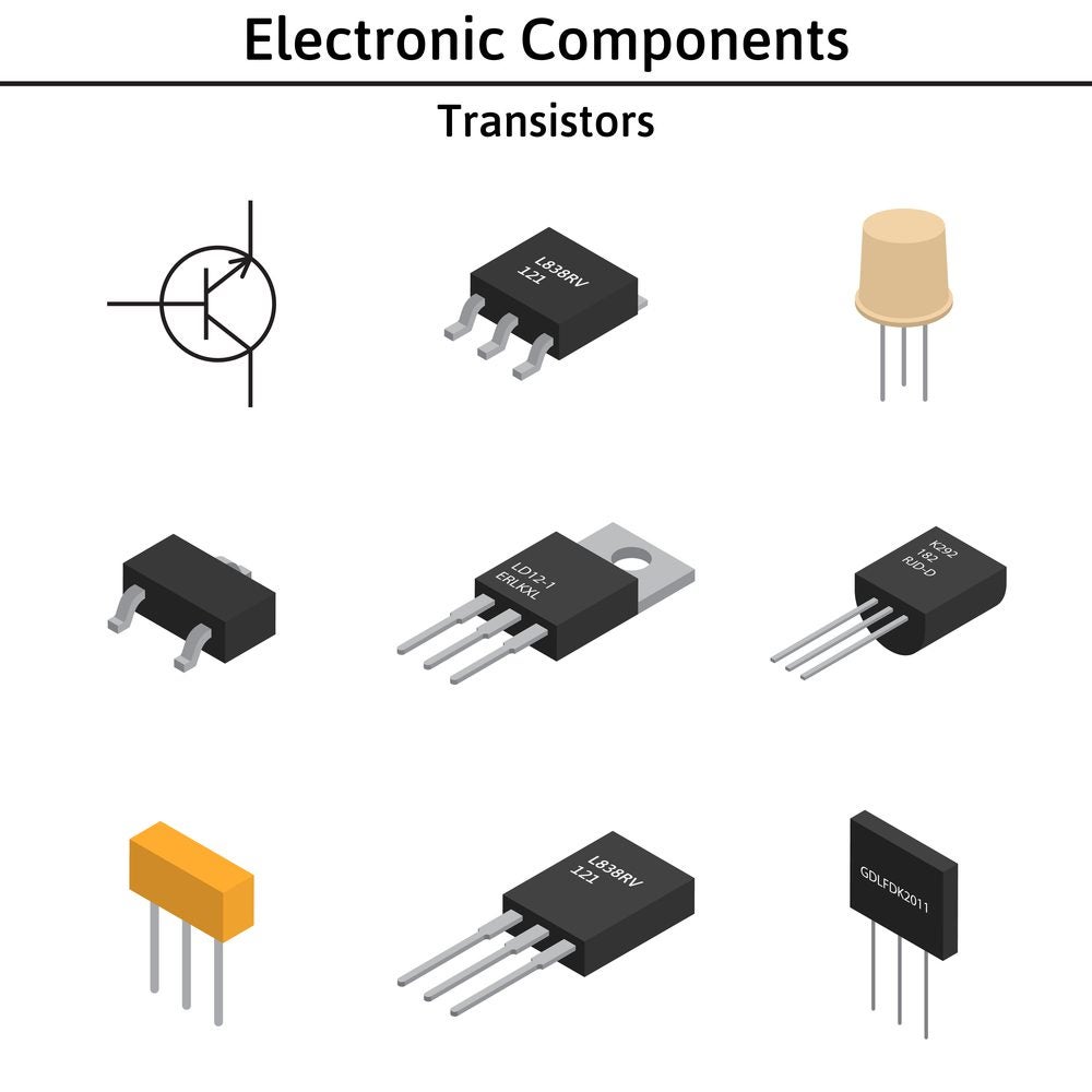
Types and Uses of Active Components
Before the widespread use of transistors, vacuum tubes were the preeminent active electronic component for many electronic devices, products, and appliances. Although the basics of operation are similar, semiconductor-based active components have several distinct advantages to their vacuum tube forefathers.
Types of Active Components
The largest group of active electronic devices are classified as semiconductor-based. Semiconductors are made primarily from silicon (Si), germanium (Ge), and gallium arsenide (GaA), and they manipulate the electrical properties of these materials for their operation. Other active component types commonly used in electronic applications are listed below. Note that this list of classification types is representative of the common uses of active electronic components. There are also many sub-categories of specific functional devices within this list that are not displayed.
Active Electronic Component Types
- Semiconductors – transistors, diodes, thyristors, ICs, optoelectronic devices
- Displays – liquid crystal display (LCD), LED display, overhead LED (OLED) display
- Power sources – power supplies, solar cells, fuel cells, Piezoelectric generators
- Vacuum tubes – Cathode Ray Tube (CRT), vacuum fluorescent tube (VFT), X-ray, klystron
How Are Active Components Used on Circuit Boards?
A good general description for an active electronic component is:
Active electronic components are discrete devices utilized to change or modify the flow of current to enable an electric circuit to exhibit a desired functionality. Typically, these components are used as any of the following:
|
As the above description indicates, active components are versatile and perform important functions. However, the successful operation of a device requires the PCB layout to accurately reflect the physical attributes of the component and makes use of good manufacturability guidelines.
PCB Layout Considerations for Active Electronic Components
Generally, circuit board layout design consists of two stages:
- Schematic generation
- Board layout
The first stage is where the symbol for each component is illustrated. For board layout, each component’s footprint is required. Creating PCB footprints from scratch, which is sometimes necessary for custom components, can be a painstaking process wrought with opportunities for error. A much better option is to utilize a CAD library, such as the one shown in the figure below, for component selection.
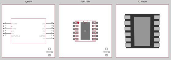
The figure above shows the CAD library images, symbol, footprint, and 3D model for a commonly used diode controller from Texas Instruments. This information is necessary to generate the schematic and lay out the active component on the circuit board. During PCB layout, the designer must address manufacturability concerns for the contract manufacturer (CM) to build the board accurately.
PCB Layout Considerations for Active Electronic Components
In most cases, a CM must rely on design files and the BOM to build a PCBA. Therefore, it is essential for these files to accurately reflect design intent, which means addressing specific manufacturing issues.
Manufacturing Requirements for Active Component Layout Design
- Placement and Clearances
The placement of your components matters, as it affects heat distribution and dissipation during assembly and operation. There must also be sufficient clearances between component pins, separate component footprints, and the board edge. Otherwise, solder bridges may form, resulting in short circuits, affected depanelization, or operational concerns such as stray capacitance or arcing.
- Trace Routing
Good signal integrity depends on the size, length, and location of trace routing. Consideration must also be given to limitations such as spacing between adjacent traces and like copper weights on a layer when laying out and connecting components.
- Layer Stackup
Today, most PCBs are populated with SMD packages, necessitating using vias for interconnecting traces. Designers must carefully plan each layer of the circuit board so their number, order, and type work together for proper operation. This planning must also include precise routing strategies for the various DC (power and ground), analog (RF), and digital signals from your active components to the proper layers and planes.
Meeting the manufacturing requirements above is not optional. Designers must incorporate these requirements into their PCB layouts. Your ability to meet these requirements depends upon the accuracy of your active component library. The best way to ensure your component symbol, footprint, and 3D model are correct is to acquire them from a trusted resource where you can ensure there will be no mismatch with the manufacturer’s data files.
If you’re looking for CAD models for common components or active electronic components, Ultra Librarian helps by compiling all your sourcing and CAD information in one place.
Working with Ultra Librarian sets up your team for success to ensure streamlined and error-free design, production, and sourcing. Register today for free.


")
")