
In electronics, it is common to receive weak signals that need boosting before they can be utilized. Amplifiers are the electronic devices that fill this position on printed circuit boards. There are many types of amplifiers, such as BJTs, FETs, IGBTs, and op-amps, which may be composed of the other types.
Op-amps, which are fairly simple to implement, are used for a wide range of applications. One such op-amp is the TL082A, a dual op-amp manufactured by Texas Instruments, Inc. Designers who wish to know more about this op-amp should explore the TL082ACP datasheet, which holds critical information about this versatile amplifier.
TL082A Dual Operational Amplifier Applications and Features
The TL082A dual op-amp is one of many IC amplifier components manufactured by Texas Instruments, Inc. Texas Instruments (TI) produces amplifiers for virtually any application. This selection includes the JFET input TL082 op-amp series—TL082, TL082A, and TL082H. With the release of the TL082A, the device’s offset was improved from the original base design of the TL082. Although not the latest version, this IC is used for many applications, such as:
- Inverters for solar energy systems
- Industrial power modules and motor drives
- Universal power supplies (UPSs): 1ɸ and 3ɸ
- Audio mixers
- Test equipment for batteries
As this list shows, the TL082A finds a home in production facilities, energy networks, communications systems, and the lab. The amplifier can meet the needs of these applications due to its attractive features, as shown below.
- High slew rate: 20 V/µs (TL08xH, typ)
- Low offset voltage: 1 mV (TL08xH, typ)
- Low offset voltage drift: 2 µV/°C
- Low power consumption: 940 µA/ch (TL08xH, typ)
- Wide common-mode and differential voltage ranges
- Common-mode input voltage range includes VCC+
- Low input bias and offset currents
- Low noise: Vn = 18 nV/√Hz (typ) at f = 1 kHz
- Output short-circuit protection
- Low total harmonic distortion: 0.003% (typ)
- Wide supply voltage: ±2.25 V to ±20 V, 4.5 V to 40 V
The information above is just a small part of the critical data and information available from the TL082ACP datasheet.
How to Effectively Use the TL082ACP Datasheet
The TL082A is not an exceptionally complicated device. However, it is best to be familiar with its datasheet, as it includes important dimensional data and operational information that can help designers determine when and how to utilize this versatile amplifier module best.
Understanding the Architecture and Operation of the TL082A
In the figure below, the pinout is shown for the TL082A. As indicated, the package includes dual amplifiers that share power (Vcc+) and ground (Vcc-) connections.
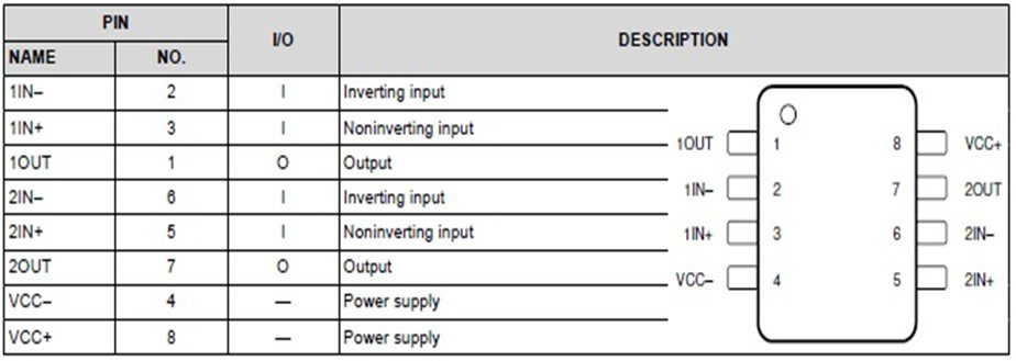
TL082A pinout and pin descriptions
The TL082A is similar in architecture to the LM741—probably the most used op-amp—as it comprises many active components, primarily transistors. However, the LM741 includes a BJT differential input network, while each amplifier of the dual channel TL082A accepts input signals for processing through an FET differential network.
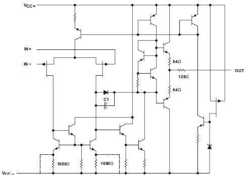
Block diagram of TL082A (each op-amp)
The PCB diagram above illustrates the operation of TL082A amplifiers. This device offers a cost-effective solution for many applications where a good slew rate, offset control, high voltage processing, and/or high gain of weak signals is required. This device can also be operated as a single (one Vcc tied to the ground) or dual supply device.
Knowing Important Device Parameters and Limitations
In addition to providing the architecture and explaining the operation of the TL082A amplifier, the TL082ACP datasheet also includes important device parameters, as listed below. This allows designers to compare it with alternative candidates for their design.
| TL082A PARAMETERS | |
| Parameters | Values |
| Number of channels (#)
Total supply voltage (Max) (+5V=5, +/-5V=10) Total supply voltage (Min) (+5V=5, +/-5V=10) Rail-to-rail GBW (Typ) (MHz) Slew rate (Typ) (V/us) Vos (offset voltage @ 25 C) (Max) (mV) Iq per channel (Typ) (mA) Vn at 1 kHz (Typ) (nV/rtHz) Operating temperature range (C) Offset drift (Typ) (uV/C) Input bias current (Max) (pA) CMRR (Typ) (dB) Output current (Typ) (mA) Architecture |
2
30 7 In to V+ 3 13 6 1.4 18 0 to 70 18 200 86 10 FET |
The parameters above, along with the constraints listed below, inform where and how designers can use the TL082A in their design.
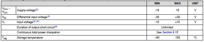
Operational constraints for the TL082A
If an increased capability is needed, consider the TL082AH as an alternative. This device is specifically designed to provide better performance for high-speed applications.
Designing With the TL082A Dual Op-Amp
There are a few tips designers should follow to create the best design for TL082A: .
Tip #1: Choose the Most Appropriate Package
The TL082A comes in different package options, which are shown in the table below.
| Package Type | Footprint Dimensions |
| 8-pin PDIP (TL082ACP) | 9.81 mm x 9.43 mm |
| 8-pin SOP | 6.2 mm x 7.8 mm |
| 8-pin SOIC | 3.91 mm x 4.9 mm |
As shown above, IC packages vary significantly, therefore, the PCB footprints needed will affect the board layout design.
Tip #2: Employ Trace Routing and Layout Best Practices
There are several trace routing and PCB layout best practices users should follow to ensure the best operation and performance of their design. These include the following recommendations from the TL082ACP datasheet:
- Use bypass capacitors to reduce EMI.
- Connect low impedance, 0.1-μF ceramic bypass capacitors between each supply pin and ground.
- Place bypass capacitors as close to the module as possible.
- For single power supply operation, add one capacitor between V+ and ground.
- Place the gain and feedback resistor(s) and other external parts close to the IC module.
- Use separate ground planes for analog and digital circuitry.
- Put as much space between input and output traces as possible. This will help reduce parasitic capacitance.
- Input traces should be as short as possible.
- To prevent leakage currents, a guard ring is a good solution.
Tip #3: Use Accurate CAD Model Design Data and Information
The TL082ACP datasheet provides a wealth of valuable data and information to help designers with component selection, circuit design, and board layout.
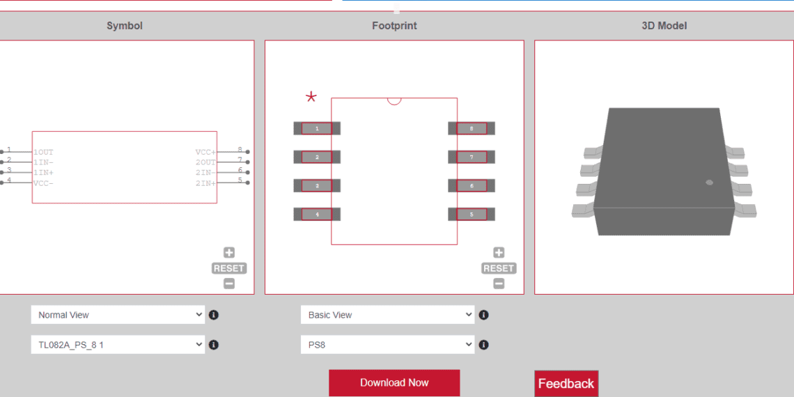
The TL082ACP schematic symbol, footprint and 3D model
Designers must also ensure that they use accurate schematic symbols, footprints, and 3D CAD models, such as shown for the TL082ACP in the figure above, from a trusted source for component information. Failing to do so may delay PCBA development due to inaccuracies that necessitate time-wasting back and forth with the CM and result in additional costs.
If you’re looking for CAD models for common components and insightful design tips that support and augment information, such as found in the TL082ACP datasheet, Ultra Librarian helps by compiling all your sourcing and CAD information in one place.
Working with Ultra Librarian sets up your team for success to ensure streamlined and error-free design, production, and sourcing. Register today for free.


")


