PCIe (Peripheral Component Interconnect Express) is a high-speed, bidirectional, point-to-point system. It is a serial bus that requires much fewer pins than a parallel bus. It is also scalable and allows for lane aggregation. Moreover, PCIe inherits a packet-based transaction protocol similar to ethernet and backward compatible with PCI.
The PCI-SIG, the community responsible for developing and maintaining PCIe specifications, has released six PCIe generations. Each generation doubles data throughput from its predecessor, offering up to 64 GT/s in PCI Gen 6. As a result, the exact PCIe routing guidelines and specifications may vary from generation to generation.
However, most techniques used with previous standards are still applicable while designing PCB with PCIe 6.0 links. Thus acknowledging an ideal board layout ensures the best signal performance in PCIe applications.
Best PCIe Routing Guidelines and Practices to Follow
Routing Path
All PCIe signals are routed together on one layer. All transmission signals are routed on the top layer, whereas all receiving signals are routed in the bottom layer. While routing very high-speed signals, traces running directly over glass fiber can have a different dielectric constant than traces running directly over epoxy. This can cause a dielectric constant mismatch between two transmission lines of the same length – known as the Fiber Weave effect. It hampers the signal quality. That’s why PCIe signals are routed following a zigzag path to mitigate the fiber weave effect’s adverse effects efficiently.
BGA Fanouts
Ideally, the exact BGA breakout depends on the pitch between the balls of a particular BGA package. Thus, it is imperative to go through its manufacturer’s datasheet for the exact fanout strategy. Partly, the escape routing also depends on the layer count. With maximum board thickness limited to 1.57mm, more layers (6+) favor the routing. Otherwise, with a 4-layer board, you’ll have a maximum of two layers for routing, with the rest preserved for internal copper planes.
Stitching Vias and Via Shielding
If possible, avoid vias in PCIe designs as they can impose impedance discontinuity, leading to signal reflection and poor signal quality. In this regard, stitching vias and via shielding are helpful.
Stitching vias are used when high-speed signals change lanes or layers. They must be positioned close to the vias to create a strong vertical structure throughout the board. You can further reduce crosstalk and electromagnetic interference in the signal route by placing all rows of vias in line with the signal path. This is known as via shielding or via fence.
ESD/EMI Layout
Any ESD/EMI component selected should allow flow-through routing of different signal pairs. Due to AC coupling caps, Pads add parasitic capacitance to the network and increase the impedance. Therefore, adding voids under the components through as many planes as possible is imperative to minimize losses. The overall routing for coupling capacitor, common-mode filter, and ESD protection should be optimized and as near as possible to the connector.
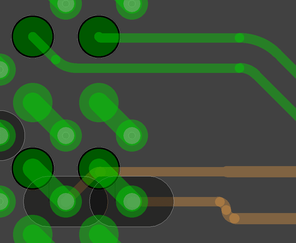
BGA Breakout Optimization
PCIe routing guidelines for BGA fanouts hold utmost importance. For a better BGA pad and via impedance matching, the design should include a large oval via anti-pads and a cutout under the BGA pad, as shown below.
Differential Board Trace Width and Spacing
The design trace width, height, and spacing should match 100Ω 20% impedance for chip-to-chip connections. If the signals are on the same PCB without any connector, you would require a closely coupled 100Ω 20% differential trace since CPUs/ASICs can tolerate a max 100-ohm impedance. It is imperative to use board stack-up material to meet this requirement.
If the application involves two adjacent differential pairs phased out or running at different data rates, there is a chance of cross-coupling. Here, the situation demands adding space between them of at least four times the dielectric height. For stripline traces, it should be three times.
Trace Length Matching and Trace Length
Differential trace length mismatch can create duty cycle distortion, resulting in reduced eye-width and compromised signal integrity. Though you will find the maximum trace length mentioned in specifications for different high-speed standards, it is important to acknowledge losses along the path. The following table shows the differential loss budget for different PCIe generations calculated at the max data rate specified.
| Generation | Loss Budget | Differential Impedance |
| Gen 1 | 13.2 dB | 100 ohms |
| Gen 2 | 16.5 dB | 85 ohms |
| Gen 3 | 20 dB | 85 ohms |
| Gen 4 | 28 dB | 85 ohms |
| Gen 5 | 36 dB | 85 ohms |
| Gen 6 | 36 dB | 105 ohms |
While planning layout and following PCIe routing guidelines, use the online CAD library of Ultra Librarian to your advantage. You can collect vital design information such as verified symbols, footprints, datasheets, CAD models and available vendors, all at one place. Working with Ultra Librarian sets up your team for success to ensure streamlined and error-free design, production, and sourcing. Register today for free.


")
")