
Among various types of transistors, JFETs (Junction Field Effect Transistors) are voltage-controlled devices that can be used as voltage amplifiers and a switch. They can also be used as choppers, phase shift oscillators, and current limiters. The 2n5457 is a low noise and high gain N-channel JFET transistor that can be used for all such applications.
However, a fair understanding of its maximum ratings, electrical characteristics, and performance curves from the 2n5457 datasheet are essential for a successful design. Therefore, before we analyze the critical elements in this transistor, let’s have some basic understanding of an N-channel junction biased field-effect transistor.
Working Principle of an N-channel JFET transistor
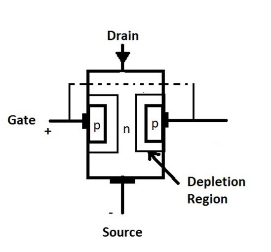
A Junction Field Effect Transistor (JFET) consists of three terminals, Gate, Drain, and Source. It can be of two types N-type and P-type. Here is the diagram of an N-type JFET.
Here the gate terminal is connected to the p substrates, whereas source and drain are connected to the n substrate. It can be seen as a combination of two PN junctions. Thus, there are depletion regions around the p substrates.
The input voltage is applied between the gate and the source. The output current is collected at the drain terminal. The best part is that it can conduct with no input supply. If the gate supply is zero and we apply a positive voltage between drain and source, enough to surpass the pinch-off voltage of the transistor, it starts to conduct current.
When the input junction is forward biased, the depletion layer decreases, and there is more current flow in the drain. The opposite happens during the reversed biased condition. With this fundamental knowledge, let’s analyze the 2n5457 datasheet.
Analyzing the 2n5457 Datasheet
Pin Out
The pin layout of the transistor is shown below.
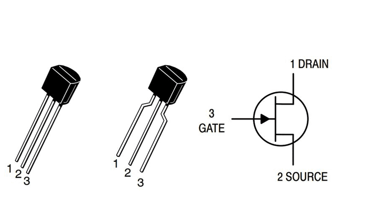
When you keep the flat space towards you, the first pin denotes the drain, the last pin denotes the gate, and the middle one is the source.
Maximum Ratings
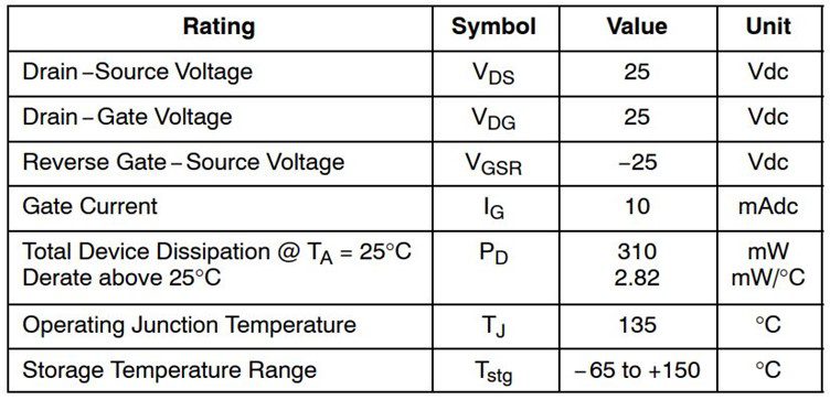 As JFET is a voltage-controlled device, you can see the maximum voltage ratings (VDS, VDG, and VGSR) are much higher than the gate current. As the gate operates at a maximum current of 10mA, the 2n5457 transistor has much higher thermal stability than any equivalent BJT transistor.
Important Technical Specifications
- Package: TO-92
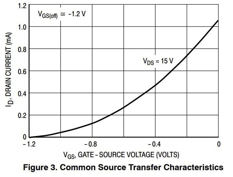
- Gate to source cut-off voltage: -0.5 to -6.0 V dc (VDS = 15 Vdc, ID = 10 nAdc)
- Zero gate voltage drain current: 1.0 to 5.0 A (VDS = 15 Vdc, VGS = 0)
- Power dissipation: 310 mW
Applications of 2n5457 N-channel Transistor
As a Switch
The 2n5457 can operate as a switch when the transistor operates in the ohmic region. 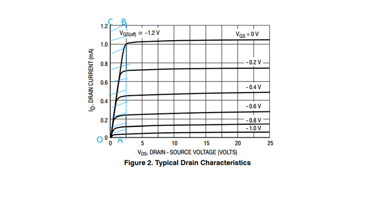 Let’s try to understand the same from the typical drain characteristics diagram as shown in the 2n5457 datasheet. The highlighted region OABC represents the ohmic region of the transistor in which it operates as a switch.
When VDS is positive and is less than the pinch-off voltage, the transistor continues to conduct current, even at zero VGS. Once we start to gradually increase VGS, the depletion layer starts to widen and narrows down the conduction channel. Consequently, the channel resistance increases up to 100 times.
We know V (voltage) = I (current) R (resistance)
For the same amount of drain current, if the channel resistance keeps on increasing, the voltage drop also increases.
Designers use this characteristic of an N-channel JFET as a variable resistor to operate the transistor as a switch.
As an Amplifier
The 2n5457 transistor can be used to amplify the input voltage by connecting a load resistor across the drain under an arrangement as shown below.
The gate-source region of the N-channel JFET is kept at a reverse potential by connecting the gate (P channel) to the negative end of the battery and the source (N channel) to the positive side of the battery. Let’s term it VGG.
The source voltage (VS) to be amplified is applied between the gate and the source terminal. Now the overall input voltage to the transistor is the sum of VS and VGG.
Before the application of AC input, VGG keeps the gate-source reversed biased. As a result, the depletion layer is high, the conduction channel is narrow, and the drain current is low.
Let’s say now we are applying the AC signal to be amplified to the input. As the input is an AC source, it will have positive and negative cycles.
During the +ve half cycle of the AC input, the gate-source junction becomes forward biased, the depletion layer decreases, and more current flows across the load resistor, leading to more voltage drop.
During the -ve half cycle of the AC input, the input junction gets reversed biased, leading to less drain current across the load resistor. However, as the depletion layer starts to build up, the resistance to the conduction path increases. So now, we get a large change in output voltage for a small change in output voltage.
You can also use the 2n5457 transistor for current limiting systems and phase-shifting oscillators as well. z
Ultra Librarian offers a huge library to access the latest 2n5457 datasheet, package dimensions, accurate footprints, ECAD/MCAD models, and application notes, all in one place. Working with Ultra Librarian sets up your team for success to ensure streamlined and error-free design, production, and sourcing. Register today for free.