
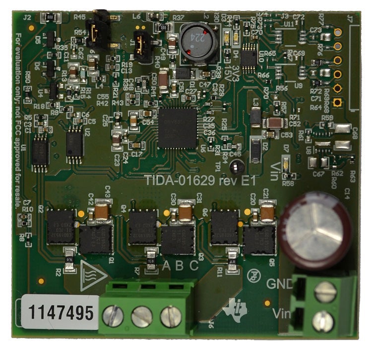
Following a good reference design guide is the best way to maximize the benefits of proven reference boards like the TIDA-01629 by Texas Instruments
Modern PCB design demands rapid time-to-market delivery while maintaining engineering excellence and cost efficiency. Reference designs provide a proven foundation necessary to accelerate development cycles, minimize design risks, and optimize resource allocation across complex electronic projects. This comprehensive reference design guide provides the strategic insights necessary to effectively leverage reference designs throughout your development process.
Reference Design Implementation Best Practices
Reference designs represent manufacturer-verified circuit implementations that demonstrate optimal component usage within specific applications. These comprehensive design packages typically include schematics, PCB layouts, bills of materials (BOMs), component libraries, and supporting documentation. By employing the best practices outlined below, you can optimize your use of these proven, time- and cost-saving resources.
| Best Practices for Implementing a Reference Design | ||
| Practice | Why It's Important | How to Implement |
| Component Obsolescence Verification | Prevents production delays and costly redesigns | Use supply chain tools to check NRND status for all components before design commitment |
| Schematic Organization | Enables efficient debugging and design iteration | Separate reference design blocks from custom circuits using hierarchical sheet structures |
| Library Validation | Eliminates manufacturing errors and assembly issues | Cross-reference all symbols/footprints against manufacturer datasheets and mechanical drawings |
| Simulation-Based Verification | Identifies functional issues before prototyping | Perform SPICE analysis on critical circuit blocks to verify expected electrical behavior |
| Layout Adaptation Strategy | Ensures form factor and performance requirements are met | Use reference layouts for guidance while creating custom arrangements for your specific needs |
| Documentation Management | Maintains design integrity across revisions | Track all modifications from baseline reference design with detailed change logs |
| Testing Protocol Development | Validates performance against specifications | Develop comprehensive test plans covering all reference design functions and custom modifications |
| Manufacturer Support Evaluation | Ensures ongoing technical assistance availability | Assess manufacturer commitment levels and available support resources before selection |
When and Why to Use Reference Designs
Choose reference designs when developing new product categories where your team lacks domain expertise or when working with unfamiliar components that require specialized knowledge. Switch-mode power supply (SMPS) designs exemplify this scenario, where switching topology selection, control loop optimization, and thermal management require extensive power electronics expertise.
High-frequency applications, such as DDR4 memory interfaces and HDMI signal routing, where signal integrity challenges can cause project delays and costly redesigns, are great candidates for reference design use. Research indicates that 90% of high-speed digital failures stem from impedance mismatches and layout errors that reference designs help prevent.
You should also consider reference designs for compliance-critical applications, where regulatory certification requirements (FCC, CE, UL) demand proven circuit topologies and layout techniques. Manufacturers invest significant resources to validate reference designs against these standards, which can be leveraged to reduce your certification risks.
Getting Started with Reference Designs
Before proceeding with a reference design, it is important to follow preliminary steps to ensure you maximize the benefits of this foundational resource for your project.
Preliminary Steps for Reference Design Usage
Step 1: Requirements Analysis and Design Selection
Begin by clearly defining your project requirements, including performance specifications, power budgets, form factor constraints, and environmental conditions. Search a comprehensive reference design library to identify designs matching your application needs.
Evaluate available reference designs based on component availability, manufacturer support levels, and design complexity. Consider both current and future product roadmaps to ensure selected components remain viable throughout your product lifecycle.
Step 2: Design Package Evaluation
Download complete reference design packages including schematics, PCB layouts, component libraries, and supporting documentation. Verify that all necessary files are available in your preferred CAD format (e.g., OrCAD, Altium, Fusion 360, KiCAD, or other supported formats).
Review the bill of materials for component obsolescence risks and supply chain considerations. Use integrated supply chain tools to identify potential sourcing issues before committing to the reference design approach.
Step 3: Schematic Integration and Customization
Import the reference design schematics into your design environment and organize circuit blocks logically. Maintain clear separation between reference design sections and custom circuitry to facilitate debugging and design iteration.
Implement necessary modifications for your specific application while preserving critical design elements that ensure proper operation. Focus customization efforts on peripheral functions rather than core circuit topologies that have undergone extensive validation.
Step 4: Component Verification and Library Validation
Perform thorough verification of all component symbols, footprints, and 3D models included in the reference design libraries. Component manufacturers occasionally include errors in reference design libraries that can cause costly manufacturing delays.
Cross-reference component part numbers with manufacturer datasheets to ensure accuracy. Identify any obsolete or discontinued components and, if necessary, replace them with suitable alternatives while maintaining electrical equivalence.
Optimizing Your Reference Design Workflow
Reference designs offer tremendous time and cost savings if implemented by following workflow efficiency optimization guidelines, as listed below.
Reference Design Guide to Workflow Efficiency Optimization
|
The guidelines can be broadly applied to any reference design implementation. However, it is advisable to understand and adhere to specific requirements that may exist for different applications. See the resources below for targeted reference design guidance based on the application.
Circuit-Specific Reference Design Applications
- SMPS Reference Designs
- DDR4 Reference Designs
- HDMI Reference Designs
Reference designs serve as essential tools for modern PCB development, providing a proven foundation that accelerates time-to-market while maintaining engineering excellence. By following established best practices and leveraging manufacturer-verified implementations, engineering teams can optimize their development workflows, reduce project risks, and deliver successful products within budget and schedule constraints.
If you’re looking for CAD models for common components or a comprehensive reference design guide, Ultra Librarian helps by compiling all your sourcing and CAD information in one place.
Working with Ultra Librarian sets up your team for success to ensure streamlined and error-free design, production, and sourcing. Register today for free.


")


