
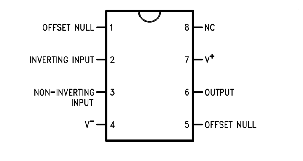
The LM741CN datasheet provides key specifications for this widely used op-amp
Few components in analog electronics are as enduring as the LM741. Introduced in the late 1960s, it quickly became the standard for general-purpose operational amplifiers, and the LM741CN variant continues to see use in production designs where dependable operation matters most. With a slew rate of about 0.5 V/µs and a gain-bandwidth product near 1 MHz, it provides a balance of simplicity and flexibility that newer op amps often trade for speed or precision.
The LM741CN datasheet remains the definitive reference for applying the device correctly. By studying its specifications, pin configuration, and design limits, engineers can achieve reliable performance whether developing new analog stages or maintaining existing systems that still depend on this benchmark amplifier.
LM741CN Datasheet – Key Specifications and Electrical Characteristics
The most important details in a component datasheet are the electrical characteristics, since they define how the device performs under real operating conditions. In the case of the LM741CN, these specifications guide engineers in predicting circuit behavior, from input performance to output drive capability, and provide limits that help ensure stable design choices.
While the LM741CN is not optimized for high speed or very-low noise, its predictable limits make it reliable in standard analog applications. By reviewing its supply requirements, input and output ranges, and small-signal behavior, engineers can quickly determine whether the device meets the needs of a given project.
| Key Specifications and Electrical Characteristics | ||||||
| Parameter | Symbol | Test Conditions | Min | Nominal | Max | Units |
| Supply Voltage | Vcc | Dual supply ±15 V | ±10 | ±15 | ±22 | V |
| Input Offset Voltage | Vio | Vs = ±15 V, 25°C | – | 2 | 6 | mV |
| Input Bias Current | Ib | Vs = ±15 V, 25°C | – | 80 | 500 | nA |
| Input Offset Current | Iio | Vs = ±15 V, 25°C | – | 20 | 200 | nA |
| Open-loop Voltage Gain | Av | RL ≥ 2 kΩ, Vout ±10 V | 20 | 200 | – | V/mV |
| Slew Rate | SR | Vs = ±15 V | – | 0.5 | – | V/µs |
| Gain Bandwidth Product | GBW | Vs = ±15 V | – | 1 | – | MHz |
| Output Voltage Swing | Vout | RL = 2 kΩ, Vs = ±15 V | ±10 | ±12 | – | V |
| Supply Current (Quiescent) | Iq | No load | – | 1.7 | 2.8 | mA |
| Operating Temperature Range | Ta | – | 0 | 25 | 70 | °C |
LM741CN Pinout and Pin Configuration
Applying the LM741CN effectively starts with understanding its pin functions in the standard 8-pin dual-in-line package (DIP). Each connection has a specific role in circuit operation, from supplying power and routing input signals to delivering the output and adjusting offset errors. A defining feature of the LM741CN is the presence of offset null pins (1 and 5), which allow designers to reduce input offset voltage by adding a trimming potentiometer.
| Pinout and Pin Configuration | |||
| Pin Num | Pin Name | Function | Application |
| 1 | Offset Null | Offset adjustment input | Connect to a potentiometer (typically 10–20 kΩ) between pins 1 and 5 to minimize input offset voltage. |
| 2 | Inverting Input (–) | Signal input | Provides the negative terminal for differential input. Used in both inverting and non-inverting configurations. |
| 3 | Non-inverting Input (+) | Signal input | Provides the positive terminal for differential input. Reference or input signal is applied here. |
| 4 | V– (Negative Supply) | Power supply | Usually connected to –15 V. Can be tied to ground in single-supply operation. |
| 5 | Offset Null | Offset adjustment input | Used with pin 1 for offset trimming. |
| 6 | Output | Amplifier output | Delivers the op amp output. Can source or sink limited current, typically into loads ≥2 kΩ. |
| 7 | V+ (Positive Supply) | Power supply | Usually connected to +15 V. Provides headroom for output swing. |
| 8 | NC (No Connect) | Not internally connected | Left unconnected in most designs. Sometimes used as a tie point on PCBs. |
LM741CN Application Circuits and Design Considerations
Beyond specifications, the real value of the LM741CN comes from how the op-amp performs in working circuits. Its design makes it suitable for learning environments and prototype stages, where engineers need a dependable amplifier that tolerates imperfect layouts or component choices.
Common application circuits
- Inverting amplifier – In this configuration, the input signal is applied to the inverting terminal through a resistor, while the non-inverting terminal is tied to ground. The gain is determined by the ratio of the feedback resistor to the input resistor. This arrangement is popular in sensor conditioning and instrumentation, where a known scaling factor is required.
- Non-inverting amplifier – Here, the input signal is applied to the non-inverting terminal, and the gain is always greater than one. The circuit provides a high input impedance, making it suitable for buffering weak signals before further processing stages.
- Summing amplifier – By feeding multiple input signals into the inverting terminal through separate resistors, the LM741CN can act as a weighted summer. This circuit is common in audio mixers, signal combining systems, and analog computation tasks.
- Integrator and differentiator – With a capacitor placed in the feedback path, the LM741CN can perform mathematical integration of the input signal. By swapping the capacitor into the input path, the device operates as a differentiator. These circuits are useful in waveform generation, filters, and analog controllers.
Design considerations for engineers
Every circuit has limits, and the LM741CN is no exception. The slew rate, typically around 0.5 volts per microsecond, confines its use to low- and mid-frequency applications. While the device can be powered from a single supply, it achieves its best performance with dual rails such as ±15 volts, which allow for a wider output swing.
Additionally, offset voltage and bias currents may introduce small errors, but these can be minimized by using the offset null pins with a trimming potentiometer. Although the LM741CN is tolerant of output short circuits, long-duration shorts increase thermal stress and should be avoided. Its modest gain-bandwidth product of about 1 megahertz also means it is best suited for stable, low-frequency designs rather than high-speed signal paths.
Because of these considerations, engineers often rely on more than just the datasheet when incorporating the LM741CN into their work. Access to accurate CAD models, verified specifications, and sourcing information helps reduce errors and speed up the design process.
If you are looking for CAD models for common components or for the LM741CN datasheet, Ultra Librarian helps by compiling all your sourcing and CAD information in one place. With access to popular ECAD applications and worldwide distributors, Ultra Librarian makes it easier to bring designs from concept to production.
Working with Ultra Librarian sets up your team for success by ensuring streamlined and error-free design, production, and sourcing. Register today for free.


