
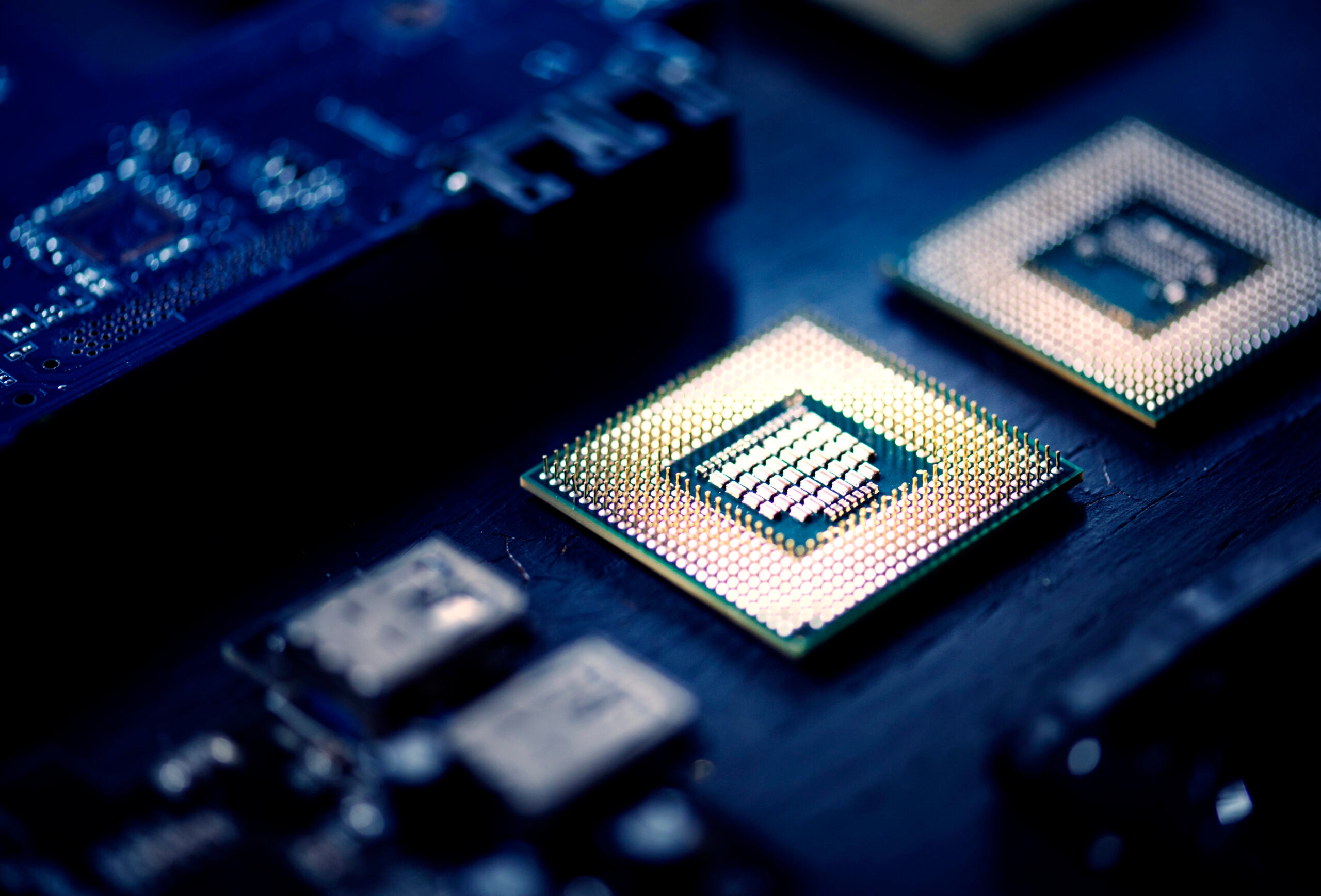
Gallium Nitride (GaN) semiconductor chip on a circuit board.
The demand for smaller, faster, and more efficient power systems is driving engineers to look beyond the limits of traditional silicon. Gallium nitride has emerged as a breakthrough semiconductor material, capable of handling higher voltages, achieving faster switching speeds, and operating at elevated temperatures. Its unique characteristics allow devices to deliver greater power density and efficiency while maintaining reliability in demanding environments.
For design engineers, understanding GaN material properties is key to choosing components that meet modern performance and requirements. By examining how this material behaves under electrical and thermal stress, engineers can make informed decisions about where it fits best in their designs.
Understanding GaN Material Properties
Gallium nitride is classified as a wide bandgap semiconductor, as it requires more energy to move electrons from the valence band to the conduction band compared to materials like silicon. This property, quantified by its bandgap energy of about 3.4 electronvolts, enables GaN to withstand stronger electric fields before breakdown occurs. As a result, GaN devices can operate safely at higher voltages and temperatures, giving engineers more flexibility in designs.
Another material characteristic is GaN’s high breakdown field strength, typically around 3.3 megavolts per centimeter. This allows the material to resist electrical failure even under substantial voltage stress. When combined with its high electron mobility and saturation velocity, GaN can transfer charge carriers more quickly through the lattice, enabling rapid switching performance that supports the development of smaller and faster electronic components.
Thermal performance also plays a role in GaN’s appeal. The material’s high thermal conductivity, measured between 130 and 230 watts per meter-kelvin, allows it to move heat efficiently away from active junctions. Its strong heat capacity further enhances stability, ensuring that GaN components maintain consistent electrical behavior under continuous or high-load operation.
These physical and electronic characteristics determine GaN’s behavior under demanding electrical and thermal conditions, as summarized below.
Applications of GaN Technology
The transition from silicon to gallium nitride began in the early 2000s as power and frequency demands increased beyond the capabilities of conventional materials. Initially adopted in RF and radar systems, GaN’s efficiency soon led to widespread use in consumer electronics, automotive power systems, renewable energy, and industrial infrastructure.
Power Conversion Systems
Power conversion is one of the most notable areas where GaN devices outperform conventional silicon. Their ability to handle higher voltages and switch faster enables more efficient AC-DC and DC-DC converters with smaller magnetic components. In systems such as consumer chargers, industrial power supplies, and data center modules, GaN transistors minimize conduction losses, helping designers achieve high power density while reducing cooling requirements.
RF and High-Frequency Applications
GaN’s wide bandgap and high electron mobility make it ideal for radio frequency and microwave designs. It supports higher power outputs and greater efficiency at frequencies exceeding 10 GHz, enabling advancements in radar, satellite communication, and 5G infrastructure.
GaN amplifiers deliver strong signal integrity and linearity even under demanding thermal and electrical loads, which is essential for maintaining precision and range in telecom systems. These characteristics allow RF engineers to design more compact and powerful transmitters for both commercial and defense use.
Renewable Energy and Power Infrastructure
Renewable energy systems benefit from GaN’s high efficiency and voltage tolerance. Inverters used in solar, wind, and energy storage applications leverage GaN transistors to convert power with reduced loss and improved thermal control. The result is more efficient energy transfer and lower maintenance requirements over time. In grid-tied or distributed power applications, GaN’s fast switching speed enables real-time power conditioning, ensuring stable output and reduced harmonic distortion.
Aerospace and Industrial Equipment
GaN’s radiation resistance and high-temperature tolerance enable reliable performance in avionics, satellites, and remote sensing equipment. In industrial motor drives or robotics, GaN helps improve control precision and efficiency, reducing system weight while maintaining mechanical stability.
Electric Vehicles and Automotive Systems
In electric and hybrid vehicles, GaN devices are increasingly replacing silicon components in traction inverters, onboard chargers, and DC-DC converters. Their higher switching frequency reduces the size of passive components, leading to lighter and more efficient powertrains. Additionally, GaN’s strong thermal stability supports operation in the high-temperature environments common to automotive systems.

EV charger using GaN power technology.
Design Considerations for GaN Components
When integrating GaN devices into a circuit, their electrical and thermal characteristics introduce design requirements that differ from traditional silicon components. Addressing these factors early helps ensure stable operation, efficient heat handling, and reliable long-term performance.
- Gate Drive Requirements: Match the gate driver capability to GaN’s fast switching behavior to prevent overshoot and ringing.
- Layout and Parasitics: Use short, low-inductance routing and strong grounding to reduce EMI and preserve switching speed.
- Power Density and PCB Strategy: Prioritize controlled current paths and thermal spreading in high-density layouts.
- Thermal Management: Implement substrates, vias, or heat spreaders to maintain stable junction temperatures.
- Packaging and Library Compatibility: Confirm device models align with ECAD libraries to streamline design and sourcing.
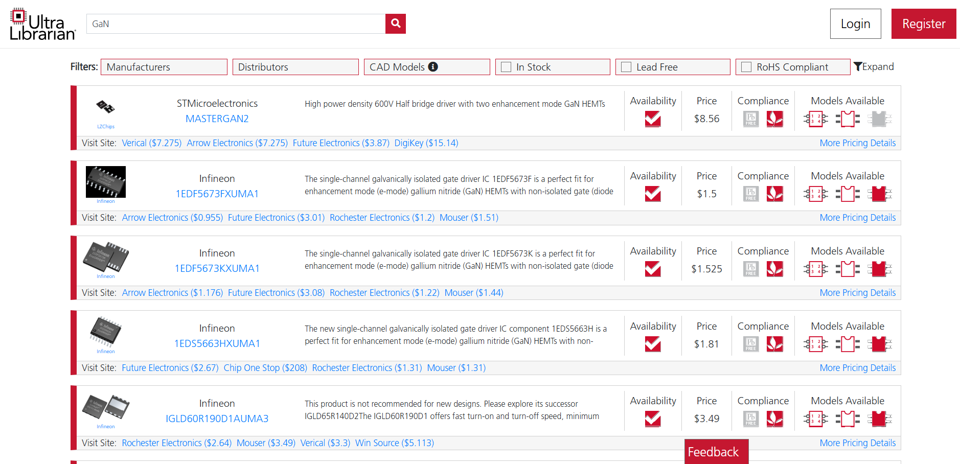
GaN component listings on Ultra Librarian.
If you’re looking for CAD models for common components or GaN material properties, Ultra Librarian helps by compiling all your sourcing and CAD information in one place. Explore popular ECAD applications, find components from worldwide distributors, and simplify every stage of your workflow, from schematic design to final assembly.
Working with Ultra Librarian sets up your team for success by ensuring streamlined and error-free design, production, and sourcing. Register today for free.


")
")