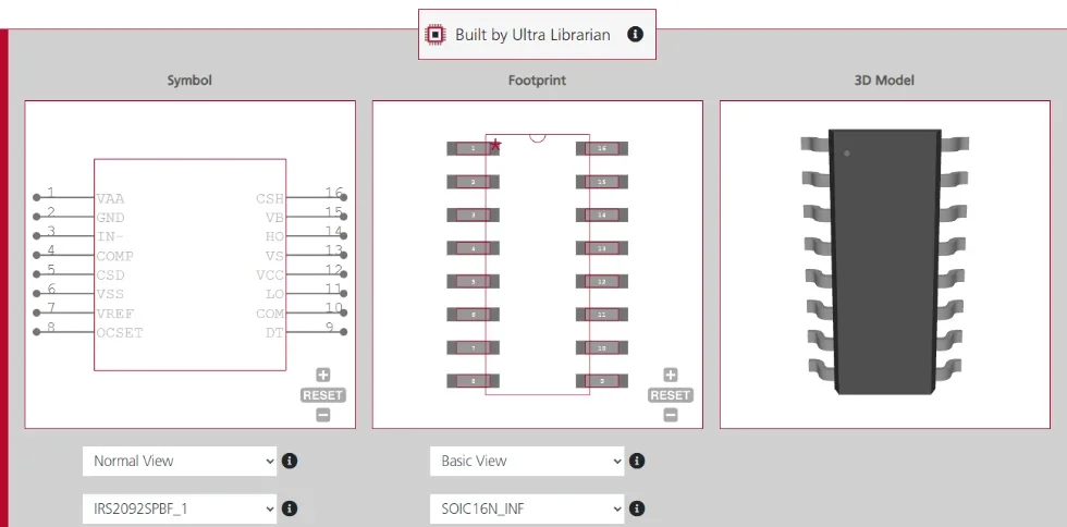
IRS2092S Symbol, Footprint, and 3D Model featured on Ultra Librarian
Class D amplification has revolutionized the audio industry, allowing for massive power output in compact form factors. However, designing high-fidelity Class D amplifiers often presents a choice: sacrifice audio quality for the simplicity of an “all-in-one” chip, or struggle with the complexity of discrete component designs. The Infineon IRS2092S bridges this gap. It is a high-voltage, high-performance protected digital audio amplifier driver with an integrated pulse width modulator.
By pairing the IRS2092S with external MOSFETs, engineers can scale power output from 50W to 500W while maintaining the audio performance expected of high-end audio systems. For designers aiming to build advanced home theater systems, active subwoofers, or professional audio gear, mastering the IRS2092S datasheet is essential. This guide breaks down the critical specifications, pinout architecture, and operational theory found in the documentation.
Understanding Class D Amplification
To appreciate the capabilities of the IRS2092S, it is helpful to understand the topology it drives. Unlike traditional Class AB amplifiers, which operate output transistors in their linear region (acting essentially as variable resistors), Class D amplifiers operate as switches. In a Class D topology, the output transistors are driven to be either fully ON or fully OFF:
- When ON: The current is high, but the voltage drop across the transistor is near zero.
- When OFF: The voltage is high, but the current is zero.
Since Power = Voltage × Current, the power dissipated as heat in the transistors is minimal in both states. This enables Class D amplifiers to achieve efficiencies of up to 90%, significantly reducing the need for bulky heat sinks and allowing for high-power audio in compact packages.
The Role of Pulse Width Modulation (PWM)
Class D amps work by converting the incoming analog audio signal into a high-frequency square wave through Pulse Width Modulation (PWM). The width of the pulses over a given time corresponds to the amplitude of the audio signal. This switching signal is amplified and then passed through a passive LC (Inductor-Capacitor) low-pass filter, which removes the high-frequency switching noise and reconstructs the original analog audio signal for the speaker.
While the concept is simple, the execution is difficult. Precise control of switching timing, dead-time, and feedback is required to minimize distortion. The IRS2092S integrates such complex control functions into a single chip.
IRS2092S Datasheet: Key Specifications
The IRS2092S is distinct because it is not just a gate driver; it is a self-oscillating PWM modulator combined with a high-voltage gate driver. This architecture allows the system to operate without an external clock, reducing EMI and component count. The device also integrates critical protection features that are often complex to implement discretely, such as Over-Current Protection (OCP) and dead-time generation.
Key Technical Specifications
| Feature | Value / Range |
| Topology | Class D Half-Bridge Driver |
| Supply Voltage (Vcc) | 10V to 18V |
| Floating Supply (VB) | Up to 220V |
| Output Sink/Source Current | 1.2 A / 1.0 A |
| Oscillation Frequency | Up to 800 kHz |
| Selectable Deadtime | 25, 45, 75, or 105 ns |
| Audio Performance | 0.01% THD+N |
Pin Configuration and Functions
The IRS2092S utilizes a standard surface-mount SOIC-16 package. A critical feature of the device is the floating input structure, which simplifies half-bridge implementations.
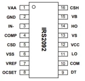 Pin configuration diagram of the IRS2092S (Top View).
IRS2092S Pin Descriptions
| Pin # | Name | Function | Description |
| 1 | VAA | Floating Input Supply | Positive supply for the floating input section (typically +5V relative to GND). |
| 2 | GND | Input Return | Return (ground) reference for the floating input supply. |
| 3 | IN- | Analog Input | Inverting analog input (audio signal input). |
| 4 | COMP | PWM Output | Phase compensation / Comparator input. |
| 5 | CSD | Protection | Shutdown timing capacitor. Controls overload protection delay, and self-reset timing. |
| 6 | VSS | Floating Input Supply | Negative supply for the floating input section (typically -5V relative to GND). |
| 7 | VREF | Reference | 5V reference output for setting OCP thresholds. |
| 8 | OCSET | Protection | Low-side over-current threshold setting. |
| 9 | DT | Configuration | Input for programming deadtime (voltage-based). |
| 10 | COM | Power Ground | Low-side supply return (Ground for the power stage). |
| 11 | LO | Output | Low-side gate drive output. |
| 12 | VCC | Power Supply | Low-side logic and gate drive supply (10V-18V). |
| 13 | VS | Output | High-side floating supply return (connected to the switching node). |
| 14 | HO | Output | High-side gate drive output. |
| 15 | VB | Power Supply | High-side floating supply voltage (referenced to VS). |
| 16 | CSH | Protection | High-side over-current sensing input. |
Functional Block Diagram and Operation
The architecture of the IRS2092S is based on a self-oscillating PWM modulator. Unlike traditional Class D controllers, which require a fixed-frequency triangle wave generator, the IRS2092S oscillates based on the propagation delay through its internal blocks and the external LC filter feedback. Ideally suited for high-fidelity audio, this architecture allows the high-current gate-drive stage and the sensitive, low-noise error amplifier to reside on a single silicon die through proprietary noise-isolation technology.
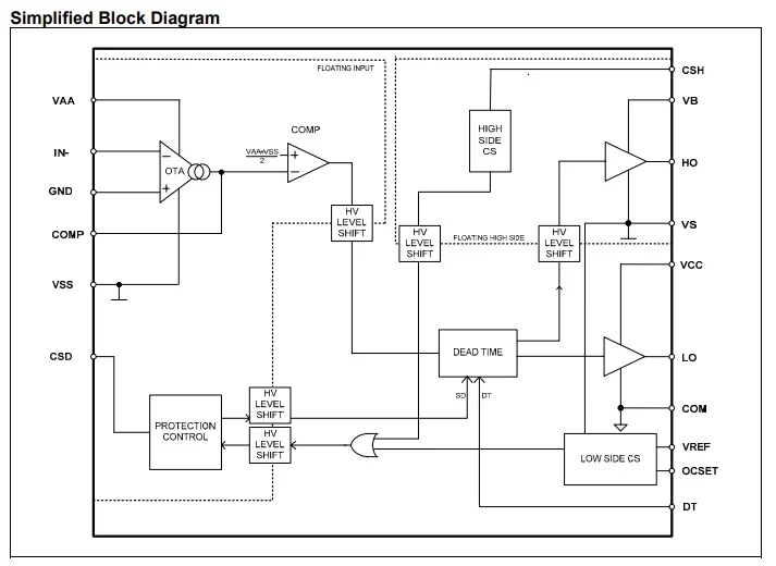 Functional block diagram from the IRS2092S datasheet.
Key Functional Blocks and Workflow:
- Analog Front End (Floating Input): The input stage is powered by floating supplies (VAA/VSS) for maximum noise immunity. It features an Operational Transconductance Amplifier (OTA) that acts as the error amplifier. The OTA sums the analog input audio (IN-) and the feedback signal from the switching node.
- PWM Modulation: The OTA integrates the error, and the internal PWM Comparator monitors this signal against a reference voltage [(VAA+VSS)/2]. When the error exceeds the threshold, the comparator switches, generating the Pulse Width Modulated signal without the need for an external clock.
- Level Shifting and Deadtime: The PWM signal passes through high-voltage Level Shifters to cross from the floating input domain to the driver domains. The Dead Time block then generates complementary outputs for the high and low sides, inserting a programmable delay (configured via the DT pin) to prevent shoot-through currents where both MOSFETs might conduct simultaneously.
- Bidirectional Protection: The diagram illustrates two distinct current sensing mechanisms for robust protection.
- High Side CS: Monitors the CSH pin relative to the high-side supply (VB) to detect over-current events in the top MOSFET.
- Low Side CS: Uses the OCSET pin and an internal voltage reference (VREF) to monitor the bottom MOSFET.
- Both sensors feed into the central Protection Control logic, which manages the shutdown sequence via the CSD pin.
- Feedback Loop: The control loop is closed by taking the switching node voltage (or the post-filter voltage) back to the input. This continuous feedback ensures the output reproduces the input audio while correcting for power supply fluctuations and stage non-linearities.
The Infineon IRS2092S is advantageous to engineers designing for the audio industry because it eliminates the complexity of building a discrete modulator for high-power Class D designs, while allowing the flexibility to choose external MOSFETs tailored to the specific power requirements of the project.
If you’re looking for verified CAD models for the IRS2092S datasheet, Ultra Librarian helps by compiling all your sourcing and CAD information in one place. Our platform provides verified, ready-to-use footprints, symbols, and 3D models that support all popular ECAD applications, along with sourcing information from worldwide distributors.
Working with Ultra Librarian sets your team up for success, ensuring streamlined and error-free design, production, and sourcing. Register today for free.