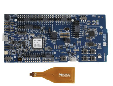
Nordic Semiconductor NRF52840 Development Kit
The nRF52840 datasheet from Nordic Semiconductor details a 2.4-GHz system-on-chip (SoC) designed for multiprotocol wireless applications. The device combines a 64-MHz ARM Cortex-M4F processor, 1 MB of flash, 256 kB of RAM, and a broad radio feature set within a compact package, enabling its application in Internet of Things (IoT) nodes, wearable and consumer devices, industrial sensors, smart home controllers, and embedded peripherals. In this article, we’ll examine key product specifications of the nRF52840.
nRF52840 Core Architecture
The nRF52840 SoC integrates an ARM Cortex-M4 32-bit processor with a floating-point unit (FPU), running at 64 MHz. The FPU supports single-precision arithmetic in hardware, which facilitates the implementation of sensor fusion, control loops, digital filtering, or any workload that relies on repeated floating-point operations.
Cortex-M4F core capabilities include:
- Digital Signal Processing (DSP) instructions: Great for tasks such as audio processing or complex sensor data filtering.
- Single-cycle multiply and accumulate (MAC) operations: Essential for fast mathematical computations.
- Hardware division: Speeds up division operations that would otherwise take many clock cycles.
- 8- and 16-bit single instruction multiple data (SIMD) instructions: Boosts throughput for parallel data processing.
In CoreMark testing, the nRF52840 reaches a score of 212 when executing from internal flash with the instruction cache enabled. This indicates performance measured under typical on-chip execution conditions, where the cache reduces wait states associated with flash reads, and reflects the device’s throughput for control-oriented workloads. The device provides 1 MB of on-chip flash memory for program storage and 256 kB of RAM for data and stack use.
Managing this memory efficiently falls to the Non-Volatile Memory Controller (NVMC). It oversees all flash operations, such as writing and erasing, although these are subject to some restrictions on cycles and methods to maintain flash integrity. The chip relies on EasyDMA, a hardware-driven direct memory access mechanism that enables peripherals to read from or write to RAM without requiring CPU intervention.
nRF52840 Connectivity Options
The nRF52840 includes a 2.4-GHz multiprotocol radio transceiver that supports several wireless standards and data-rate modes:
- Bluetooth 5 Compatibility: Supports 1 Mbps and 2 Mbps PHYs, plus coded 500 kbps and 125 kbps PHYs.
- Use cases: 1 Mbps for standard BLE peripherals; 2 Mbps for high-throughput, short-range applications (e.g., audio bridges, HID devices); coded PHYs for extended range and reliable links in RF-dense environments.
- IEEE 802.15.4-2006 Support: Operates at 250 kbps for Thread and Zigbee networks.
- Use cases: Mesh networks with self-healing behavior, IPv6-enabled devices, or applications requiring interoperability with Thread/Zigbee ecosystems.
- Nordic’s Proprietary 2.4 GHz Modes: Offers 1 Mbps and 2 Mbps operation with low protocol overhead.
- Use cases: Deterministic point-to-point links, low-latency sensors, or remote controls where BLE stack overhead is unnecessary.
Heading for Performance and NFC Capabilities
The radio offers the following performance specifications:
- Receiver Sensitivity: It includes a strong -95 dBm in 1 Mbps Bluetooth Low Energy (BLE) mode. For extreme long-range needs, it reaches an even more remarkable -103 dBm in 125 kbps BLE mode.
- Transmit Power: You can push out up to +8 dBm, adjustable down to -20 dBm in 4 dB steps. This granular control is perfect for fine-tuning range and power efficiency.
- Integrated Antenna Output: A built-in single-ended antenna output with an on-chip balun helps pare down external component count, keeping your bill of materials lean.
Beyond traditional RF, the nRF52840 integrates a Type 2 NFC-A tag, enabling short-range field detection and out-of-band communication:
- Out-of-Band Pairing: Enables convenient “touch-to-pair” functionality with NFC-enabled devices.
- Wake-on-Field Applications: The device can wake up simply by detecting an NFC field, which is handy for user-friendly setups in consumer electronics or for quick taps in industrial applications to trigger specific actions.
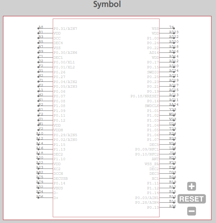
Symbol of the NRF52840-QIAA-R provided by Ultra Librarian
I/O and Peripherals Breakdown from the nRF52840 Datasheet
The nRF52840 includes a range of I/O and peripheral interfaces.
Let’s break down some of its key connectivity options:
- General Purpose I/O (GPIO) Pins: There are 48 pins, each with flexibility, and they can be individually configured for:
- Direction (input/output)
- Drive strength
- Internal pull-up or pull-down resistors
- Pin sensing (to detect high/low logic levels or any state change)
This granular control is extremely important for minimizing power consumption and effectively managing a wide array of external circuits.
- Wired Connectivity:
- USB 2.0 Full-Speed Controller: Operating at 12 Mbps, this controller is a game-changer for devices that require interfacing with a host computer for data transfer, firmware updates, or debugging.
- Quad Serial Peripheral Interface (QSPI): A 32 MHz interface for high-speed external flash memory access.
- High-Speed SPI: Operates at 32 MHz, suitable for fast communication with other peripherals.
- Audio Interfaces:
- I2S (Inter-IC Sound): Used for connecting to digital audio codecs.
- PDM (Pulse Density Modulation): Used for direct interfacing with digital microphones.
- Standard Serial Communication:
- UART/UARTE Instances: Multiple instances support EasyDMA for efficient, low-overhead data transfer.
- I2C Compatible Two-Wire Interfaces (TWI/TWIM/TWIS): Supports I2C communication for connecting sensors and other peripherals.
- Analog Sensing:
- 12-bit, 200 kSPS Analog-to-Digital Converter (ADC): Features 8 configurable channels with programmable gain, ready for diverse analog signal acquisition.
- Timing & Control:
- Pulse Width Modulation (PWM) Units: Multiple 4-channel units for controlling motors, LEDs, and other variable-power components.
- Timers: Five 32-bit timers for precise event scheduling.
- Real-Time Counters (RTCs): Three instances for keeping track of time, even in low-power states.
The nRF52840’s peripherals provide flexible connectivity and control, enabling interaction with sensors, actuators, and external devices while reducing the need for additional components. This supports efficient, multi-functional embedded designs with precise timing, high data throughput, and low power operation.
nRF52840 Package and Pinout
The nRF52840 is typically offered in a compact aQFN73 package, measuring 7 x 7 mm. Within this package, the pins balance general-purpose I/O with dedicated functions. For instance, pins like P0.10/NFC2 and P0.09/NFC1 are specifically for the NFC antenna, while SWDCLK and SWDIO are dedicated debug pins. Many pins, such as P0.31/AIN7 or P0.02/AIN0, serve as digital I/Os but can also function as analog inputs for the ADC or other analog peripherals, depending on configuration.
For optimal performance, especially in RF applications, proper PCB layout is crucial. Nordic Semiconductor provides detailed reference layouts and PCB guidelines on its website to ensure designers can meet specifications for antenna matching and decoupling. Additionally, the nRF52840 datasheet provides further information on pin assignments with individual descriptions and recommended usage for each pin.
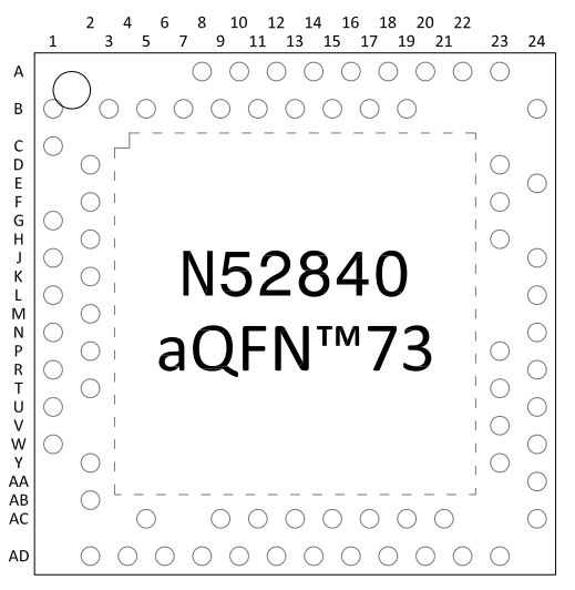
Distribution of pin types on the N52840 aQFN73 package
If you’re looking for CAD models for common components or need detailed insights from the nRF52840 datasheet, Ultra Librarian helps by compiling all your sourcing and CAD information in one place. Explore our extensive library for popular ECAD applications and easily find components from worldwide distributors.
Working with Ultra Librarian sets your team up for success, ensuring streamlined and error-free design, production, and sourcing. Register today for free.