Most engineers treat board-to-board connectors as passive mechanical components right up to the point where a design fails signal integrity (SI) validation. Past 10 Gbps, that assumption becomes expensive. At these data rates, connectors stop being simple contacts and start behaving as transmission line discontinuities, where every geometry change reflects energy back toward the source and closes the eye at the receiver. This article examines how to choose high-speed board-to-board connectors, balancing electrical parameters with mechanical resilience.
Selecting high-speed board-to-board connectors is more important now than ever, as modern protocols constantly push the physical limits of speed. For instance, PCIe Gen 4 runs at 16 GT/s per lane, doubling the throughput of Gen 3’s 8 GT/s. At those edge rates, even a minor impedance discontinuity in the connector body generates reflections that degrade bit error ratio (BER). Because of this sensitivity to reflections, a legacy connector that passed qualification at 5 Gbps will often fail at 16 GT/s without any component changes. Rather than acting as transparent physical bridges, the connector geometry, dielectric material, and pin mapping all become active participants in channel performance.
Connectors engineered for these speeds share several defining characteristics:
- Tightly controlled contact geometries to maintain uniform impedance through the mating interface
- Minimized stub lengths to avoid resonance nulls in the passband
- Low-loss dielectric housings with specified dielectric constant (Dk) and dissipation factor (Df)
- Configurable ground pinning to isolate differential pairs from adjacent aggressors
Electrical Parameters That Determine Connector Performance
Three electrical parameters determine whether a board-to-board connector passes or fails a high-speed channel: impedance, insertion loss, and crosstalk. Failing to control any of these three metrics will irreversibly degrade the link budget, rendering downstream PCB impedance controls entirely ineffective.
Protocol Impedance Targets
Impedance mismatch at the connector interface reflects signal energy back to the transmitter. This creates standing waves that corrupt the eye pattern, a time-domain visual diagram representing signal quality. When reflections narrow or “close” this eye, the receiver can no longer distinguish logical ones from zeros, causing immediate data loss. To prevent these signal reflections, designers must match the connector hardware to the system requirements. The target differential impedance of the transmission line varies by protocol, so connector selection should match the specific routing standard from the start.
Looking at specific interfaces, USB 3.x requires a differential impedance of 90 ohms (±15%), with data rates reaching 20 Gbps for USB 3.2 Gen 2×2. PCIe and 10G+ Ethernet both target 100 ohms differential. The table below summarizes the key targets and recommended pin configurations:
Target Impedance by Protocol
| Protocol | Differential Impedance | Recommended Pin Mapping |
| PCIe Gen 4/5 | 100 ohms | Ground-Signal-Signal-Ground (GSSG) |
| 10G+ Ethernet | 100 ohms | GSSG |
| USB 3.2 / USB 4 | 90 ohms (±15%) | GSSG / Full Shield |
Engineers can filter TME’s connector catalog by impedance rating to quickly identify board-to-board connectors matched to the specific protocol requirements in the table above, narrowing thousands of options down to verified high-speed candidates in seconds.
Insertion Loss
The second governing parameter is insertion loss. The system loss budget defines the total allowable signal attenuation from the transmitter to the receiver, and every connector consumes a portion of this electrical margin. Insertion loss scales with frequency and path length, so the chosen hardware must meet the specific attenuation limit for that interconnect segment.
Controlling Crosstalk
Crosstalk is the third failure mode. Near-End Crosstalk (NEXT) couples noise back toward the transmitter, while Far-End Crosstalk (FEXT) corrupts the signal at the receiver. Both are driven by proximity between adjacent signal contacts and the quality of the return-current path.
The most effective mitigation for both NEXT and FEXT is a Ground-Signal-Signal-Ground (GSSG) pin mapping. Placing ground contacts directly adjacent to each differential pair tightly couples the return current, dramatically shortening the loop area and reducing radiated coupling between pairs. If your connector’s pinout doesn’t support GSSG, treat that as a disqualifying factor for any link above 10 Gbps.
Mechanical Specifications for Industrial Environments
Industrial hardware must maintain contact continuity through sustained vibration, thermal cycling, and shock events that would destroy a consumer-grade connector within months.
When specifying hardware for harsh environments, engineers must evaluate both physical dimensions and electrical characteristics. Pitch selection represents the first mechanical constraint to evaluate. Consumer electronics favor 0.4 mm or 0.5 mm pitches for density, but industrial designs typically use 0.8 mm to 1.27 mm pitches. The wider pitch provides thicker contact beams and stronger solder joints, which are important to handle continuous vibration.
Stack height is the second variable. Industrial mezzanine connectors span a wide range, from 4 mm to 20 mm or beyond, depending on the required clearance between boards for airflow, cable routing, or component height.
For applications with persistent vibration or robotic assembly, floating-contact mechanisms are the correct choice. Floating board-to-board connectors compensate for tolerance through spring-like terminals. These terminals withstand misalignment by offering specific mechanical advantages:
- Automatic centering in all three axes to resist high levels of shock and vibration.
- Tolerance compensation of up to ±0.7 mm in the X and Y directions.
- Z-axis tolerance compensation of up to 0.6 mm.
TME stocks a wide selection of floating-contact and fixed mezzanine connectors filterable by stack height, pitch, and mating cycle rating, making it straightforward to match hardware to the specific vibration and lifecycle demands of an industrial design.
Evaluating Mechanical Package Parameters
When evaluating a mechanical package, verify these parameters against your product lifecycle requirements:
- Mating cycles: Gold plating thickness determines contact life. Be sure to specify based on the expected field service frequency
- Floating tolerance: Confirm the exact X/Y offset the connector absorbs, and ensure it covers your assembly process variation
- Wipe length: Longer wipe lengths clear surface oxidation on each mating cycle and maintain continuity through Z-axis shock
- Retention features: Solder tabs and locating pegs transfer mechanical stress away from signal pins to the housing
Connector Footprint Layout and EMI Mitigation
High-speed connectors are simultaneously a potential EMI source and a victim. Proper layout techniques around the footprint mitigate these risks directly.
The single most important layout rule is maintaining a continuous, uninterrupted ground reference plane directly beneath the connector. Any split or void in that plane forces return currents to reroute around the gap, increasing the loop inductance and creating a radiating structure. If your layer stack requires a plane split near the connector, move the connector, not the split.
Modern signal integrity connectors often integrate grounding plates or 360-degree shielding shells. When a shielding cap envelops the connector’s exterior housing, connect it to chassis ground or your digital ground plane through multiple vias placed as close to the shell as the design rules allow. Single-point grounding of a shield at these frequencies is functionally useless.
Routing Guidelines for Surface-Mount Pads
The surface-mount device (SMD) signal pads on the PCB, where the connector attaches, form a transition zone. Differential trace routing into these connector pads requires careful attention:
- Route differential pairs symmetrically into the pads to prevent mode conversion from differential to common mode
- Place ground via stitching adjacent to the connector ground pins, providing a low-impedance path to the inner reference layers
- Use anti-pads (clearances in inner ground planes) beneath surface-mount signal pads to reduce parasitic capacitance and maintain target impedance
- Keep high-speed routing away from mechanical mounting tabs to avoid capacitive coupling to chassis ground
Any intra-pair skew introduced by asymmetric routing converts differential signal content into common-mode noise. That noise has no return path and radiates directly off the connector body, causing erratic clocking precision and timing failures.
Selecting and Implementing High-Speed Board-to-Board Connectors
Translating these electrical and mechanical requirements into a working design requires two things: the right physical hardware and verified layout data.
TME (Transfer Multisort Elektronik) carries a broad portfolio of high-speed signal integrity connectors, filterable by insertion loss profile, pitch, stack height, and mating orientation. When searching TME’s catalog for ideal component substitutes or dedicated connectors targeting 10 Gbps and above, narrow the field by impedance rating first, then pitch, and finally, mechanical robustness rating for your environment.
As data rates increase, engineers often stack boards vertically using mezzanine connectors to shorten trace lengths. However, these high-density mezzanine connectors operate in constrained spaces where physical clearance between boards, surrounding components, and thermal airflow paths must all be verified before the design is committed to fabrication.
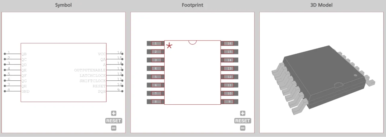
Ultra Librarian provides verified 3D STEP models for thousands of TME components. Importing a STEP model into your electronic computer-aided design (ECAD) or mechanical computer-aided design (MCAD) environment lets you confirm stack height alignment, catch component collision during mating, and map thermal relief zones accurately. Combining TME’s hardware selection with Ultra Librarian’s verified digital footprints removes the guesswork from connector integration and gives you confidence that the physical design matches the electrical intent before a single board is built.
Ready to upgrade your high-speed interconnects? Designing with board-to-board connectors shouldn’t be a guessing game. Ultra Librarian provides verified 3D models and footprints that integrate seamlessly into all popular ECAD applications, giving you easy access to components from worldwide distributors to keep your product development on track.
Working with Ultra Librarian sets your team up for success, ensuring streamlined and error-free design, production, and sourcing. Register today for free.


 If you’re looking for any of our component footprints or models, we have readily available and free options for you and your design team. Search our library for the solution you’ve been looking for.