Active power factor correction (PFC) circuits place demanding electrical and thermal requirements on power metal-oxide-semiconductor field-effect transistors (MOSFETs). Because the switching devices operate continuously at high voltage, losses generated during each switching transition can significantly affect converter efficiency and cooling requirements.
Choosing between a silicon (Si) super-junction MOSFET and a silicon carbide (SiC) MOSFET is therefore an important design decision. Effective PFC MOSFET selection requires engineers to evaluate how each device performs under the converter’s intended voltage, power, frequency, and thermal conditions.
Why Datasheets Are Not Enough for PFC MOSFET Selection
Datasheet parameters such as on-resistance, gate charge, and reverse-recovery characteristics provide essential reference points, but they do not directly show how a device will behave under a particular converter specification. Input voltage, output power, switching frequency, load, gate-drive conditions, and temperature all influence the resulting losses.
For background on PFC operation and topology selection, Toshiba’s Power Factor Correction (PFC) Circuits application note covers the relevant design fundamentals. Once those circuit requirements are established, Toshiba’s Online Circuit Simulator can be used to compare supported MOSFETs under a common set of operating conditions.
Evaluating PFC Topologies in Toshiba’s Online Simulator
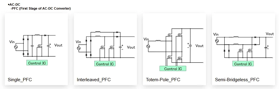
(Alt text: Four PFC circuit topologies supported by online simulator. )
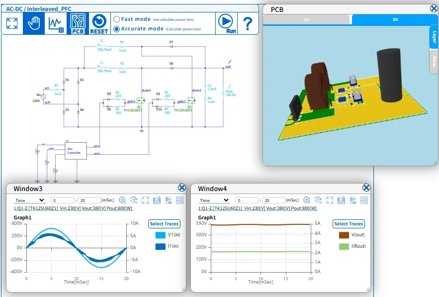
Since Ultra Librarian’s previous guide was published in March 2025, Toshiba has significantly expanded the PFC capabilities of its Online Circuit Simulator. The tool now supports Single PFC, Interleaved PFC, Totem-Pole PFC, and Semi-Bridgeless PFC, along with additional features such as printed circuit board (PCB) illustration windows and adjustable MOSFET gate-drive voltage. These updates are documented on Toshiba’s Online Circuit Simulator page.
The simulator now supports four PFC circuit topologies, each with selectable 100 V or 230 V input conditions and a 400 W to 1600 W output-power range:
- Single PFC: A conventional boost-based PFC architecture commonly used in AC-DC power supplies.
- Interleaved PFC: Uses multiple switching phases to share current, reduce input/output current ripple, and distribute power loss and thermal load in higher-power designs.
- Totem-Pole PFC: Eliminates the conventional input diode bridge from the primary conduction path, reducing conduction losses and supporting higher conversion efficiency.
- Semi-Bridgeless PFC: Reduces the number of semiconductor devices in the primary current path while retaining elements of a conventional boost PFC structure.
For this comparison, Single PFC provides a straightforward starting point for evaluating MOSFET behavior in a conventional boost PFC stage. After selecting the topology, engineers can hold the circuit specification constant while evaluating supported Si and SiC MOSFET candidates. Toshiba’s simulator narrows the available MOSFETs based on the specified circuit conditions and also provides a device search to locate additional supported parts.
The earlier Ultra Librarian article covers the simulator interface, input controls, Fast and Accurate modes, and graphical results in more detail. Here, the focus is narrower: keeping the PFC operating conditions fixed and varying the MOSFET to determine the resulting performance differences, which can inform the Si-versus-SiC decision.
Si vs. SiC: What the Simulator Reveals
Datasheets provide standardized electrical characteristics, but they do not fully predict MOSFET performance within a specific PFC converter. Two devices with similar voltage ratings and on-resistance may produce different losses once switching frequency, gate-drive conditions, temperature, and load are considered.
Toshiba’s simulator allows engineers to run the same PFC specification using supported high-voltage Si and SiC MOSFETs. Comparisons should remain within the device categories available in the tool, including supported 400 V to 900 V Si MOSFETs and applicable SiC MOSFETs. The waveform and efficiency results highlight four key differences, covered in the following subsections.
Switching-Loss Differences
Switching loss occurs when the drain-source voltage and drain current overlap during turn-on and turn-off. Although each transition is brief, the losses increase with switching frequency. The simulator lets engineers compare:
- Voltage and current waveforms
- Turn-on and turn-off behavior
- Loss waveforms and numerical loss values for each MOSFET, such as Q1 and Q2
- Numerical efficiency result
Run the Si and SiC candidates at the same PFC specification and compare the resulting voltage/current waveforms and calculated loss or efficiency results. A SiC device’s high-speed switching characteristics can reduce switching-related losses, but the simulator shows whether the theoretical advantage is meaningful at the design’s actual frequency and load.
Reverse-Recovery Behavior
Reverse recovery can increase switching loss, electrical stress, and electromagnetic interference in hard-switched PFC circuits. Simulation waveforms can reveal:
- Recovery-current magnitude
- Voltage and current stress
- Recovery-related power loss
SiC MOSFETs may offer switching-loss advantages in suitable high-voltage power conversion designs, depending on the selected topology and operating conditions.
Conduction-Loss Tradeoffs
Switching performance is only part of the decision. Engineers must also evaluate conduction loss across the expected load and temperature range. A Si MOSFET may be suitable for a lower-frequency or cost-sensitive design, while a SiC MOSFET may provide a greater benefit when switching losses, temperature, or power levels are higher. The simulator helps engineers balance both loss mechanisms rather than selecting a device based on one datasheet value.
Efficiency Across Operating Conditions
A MOSFET performing well at one load may not provide the same advantage across the full operating range. Engineers should compare minimum, nominal, and maximum load conditions where possible.
The results may show a growing SiC advantage as frequency or power increases. In other cases, a Si MOSFET may already meet the required efficiency and thermal targets. Therefore, simulation-based PFC MOSFET selection allows the decision to be based on actual converter requirements rather than general assumptions about Si and SiC devices.
How to Compare the Si and SiC Candidates
When reviewing Si and SiC simulation results, engineers should focus on the following outputs:
| Simulation result | What to evaluate | Design impact |
| Switching-loss waveform | Energy dissipated during turn-on and turn-off | Influences efficiency, device temperature, and practical switching frequency |
| Drain-source voltage and drain current | Overshoot, overlap, and switching stress | Helps identify electrical stress and potential reliability concerns |
| Reverse-recovery behavior | Recovery current and related switching effects | Influences losses, noise, and device suitability for the selected topology |
| Conduction loss | Loss while the MOSFET carries current | Affects full-load efficiency and thermal requirements |
| Efficiency curve | Performance across operating points | Shows whether the device meets system-level efficiency targets |
| Estimated device loss | Total contribution from switching and conduction | Supports heatsink and cooling-system decisions |
The objective is not simply to identify the device with the highest simulated efficiency. Engineers should determine whether the performance improvement is sufficient to affect other parts of the design.
For example, lower MOSFET losses may allow the design to use a smaller heatsink, reduce airflow requirements, increase switching frequency, or decrease the size of magnetic components. In other cases, the existing Si solution may already provide sufficient efficiency and thermal margin without requiring a change in device technology.
Turning Simulation Results Into a Device Decision
A practical evaluation should begin with a clearly defined PFC specification. Engineers can then simulate a supported Si MOSFET and a supported SiC MOSFET under the same circuit topology and operating conditions.
Simulation results remain estimates based on the available models and specified conditions. Final designs should still be validated through prototype measurements, thermal testing, and compliance testing. However, simulation can reduce the number of physical device combinations to be evaluated and help engineers enter the prototype stage with a better-supported choice of components.
From Simulation to Sourcing
Once a MOSFET has been evaluated and selected, the next step is to integrate the exact part into the PCB design. Using verified component data helps prevent footprint errors, incorrect pin assignments, and mechanical conflicts during layout and manufacturing. Engineers can search Ultra Librarian for available Toshiba computer-aided design (CAD) models, including schematic symbols, PCB footprints, and 3D STEP models.
Maintaining the same manufacturer part number across simulation, schematic capture, and PCB layout also improves traceability. The engineering team can document which device was evaluated, which operating conditions were simulated, and which physical component was ultimately placed in the design.
By combining circuit-level loss analysis with verified CAD data, engineers can make PFC MOSFET selection decisions based on both simulated electrical performance and practical design-in requirements.
Working with Ultra Librarian sets your team up for success, ensuring streamlined and error-free design, production, and sourcing. Register today for free.

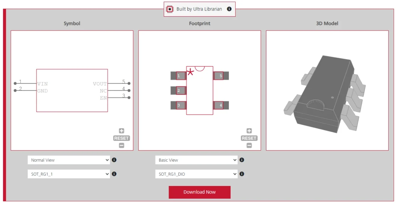
 If you’re looking for any of our component footprints or models, we have readily available and free options for you and your design team. Search our library for the solution you’ve been looking for.