Accurate power supply CAD models are critical to ensure boards meet operational and performance criteria for ECAD-MCAD systems.
Power supply PCB design demands precision in component selection, thermal management, and electromagnetic compatibility. Success depends on accurate power supply CAD models with proven layout techniques that ensure reliable operation across varying load conditions and represent real-world behavior. Reference designs provide a starting point that can significantly accelerate the design and development of your ECAD-MCAD system project.
Power Supply Component CAD Model Essentials
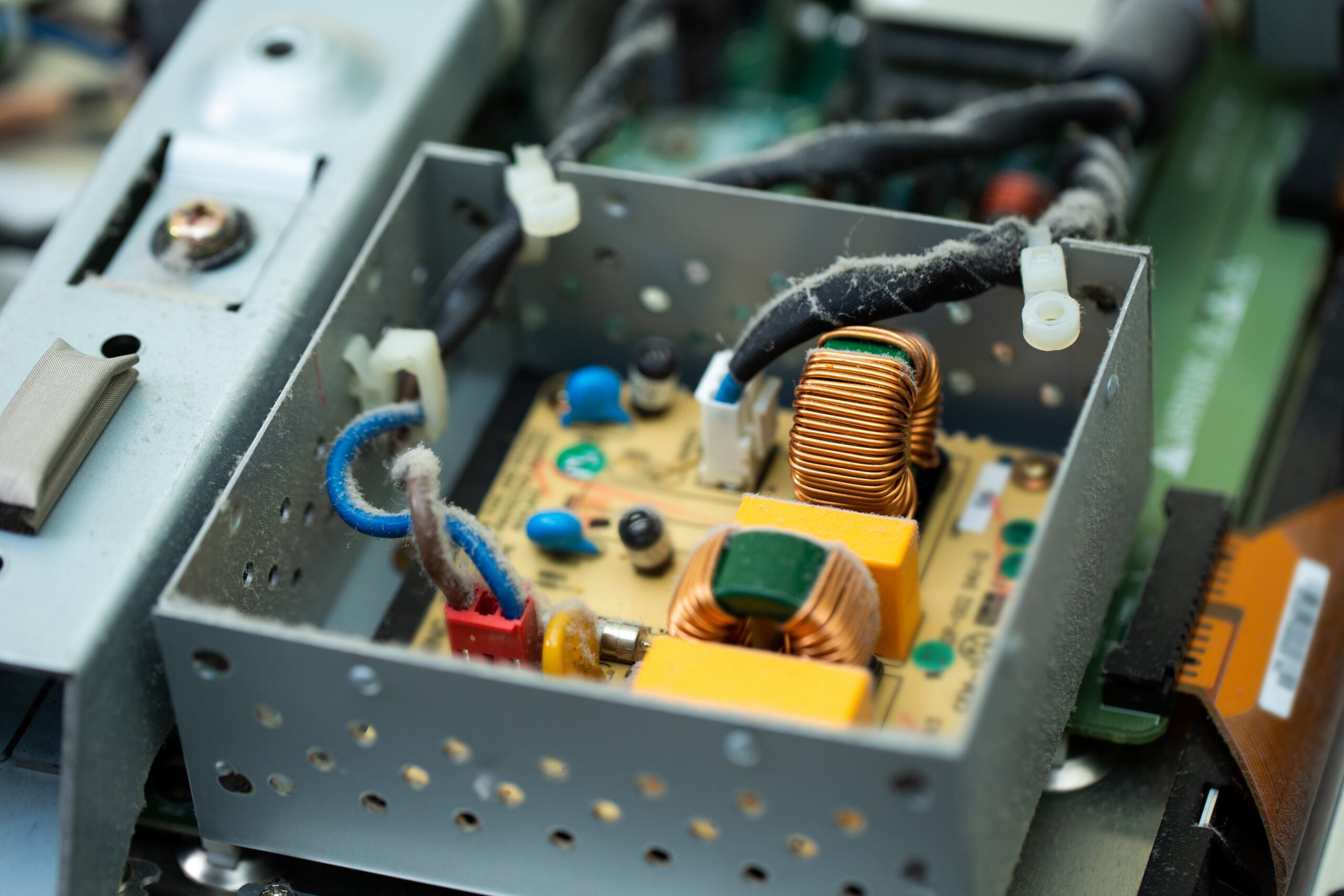
There are many types of power supply circuits; however, they fall into two major classes: linear and switch-mode power supplies (SMPS). Power supplies are responsible for ensuring that all devices and loads receive electrical energy at the required level reliably. To meet this mandate, it is essential to select the right components for your design, which will include devices from the component types listed below.
| Power Supply CAD Model Components | ||||
| Component Type | Critical Model Parameters | Typical Package Options | Thermal Considerations | Simulation Requirements |
| Switching Controllers | Pin assignments, thermal pads, package dimensions | SOIC, QFN, TSSOP | Junction-to-case thermal resistance | SPICE models for loop analysis |
| Power MOSFETs | Drain-source area, gate drive requirements | TO220, DPAK, DirectFET | Thermal via placement | Switch node parasitic modeling |
| Schottky Diodes | Forward voltage drop, reverse leakage | SMA, SMB, TO220 | Heat spreading requirements | Reverse recovery characteristics |
| Inductors/Transformers | Core material, winding resistance, saturation | Custom, standard footprints | Proximity effect modeling | Coupling coefficient accuracy |
| Output Capacitors | ESR frequency response, ripple current | 1206, 1210, radial | Self-heating at high frequency | Impedance vs frequency data |
| Input Capacitors | Voltage derating, lifetime curves | Electrolytic, ceramic, film | Ambient temperature impact | Ripple current handling |
| Feedback Components | Precision resistor matching, stability | 0603, 0805, 1% tolerance | Temperature coefficient | Noise contribution modeling |
| Protection Circuits | Response time characteristics | SOT23, SC70 | Current density limits | Fault condition behavior |
Effective power supply design requires attention to both individual component models and system-level interactions.
Optimizing Power Supply CAD Model Usage Guidelines
Ensuring your power supply will satisfy its operational and performance requirements begins with an accurate power supply CAD that represents the physical behavior of the system of integrated components. This is achievable by following CAD model guidelines and employing best practices for PCB layout, as discussed below.
Power Supply CAD Model Optimization Guidelines
- Verify the accuracy of the thermal model by comparing junction-to-ambient thermal resistance values against datasheet specifications and confirm that thermal via patterns match recommended layouts.
- Follow component library best practices to incorporate the latest package variants, revised footprints, and improved simulation models from manufacturers.
- Implement consistent naming conventions for power supply components using standard reference designators (U for controllers, S for switches, L for inductors, C for capacitors).
- Include 3D models for ECAD-MCAD design and mechanical verification to identify clearance issues with heatsinks, connectors, and adjacent circuits early in the design phase.
- Validate footprint dimensions against multiple datasheet sources and physical samples to prevent assembly issues with critical power components.
- Maintain separate libraries for different power levels and applications (low-power DC-DC, high-current supplies, isolated converters) to improve design reuse.
- Document component substitution guidelines within CAD libraries to facilitate design variants and cost optimization without compromising performance.
- Integrate thermal simulation data directly into component models to enable accurate hot-spot prediction and heatsink sizing during layout.
Layout Considerations for Power Supply Components
Power supply PCB layout significantly impacts efficiency, EMI performance, and thermal management. Component placement and routing techniques must accommodate high-frequency switching currents and minimize parasitic effects. Important layout guidelines are as follows.
| Critical PCB Supply Component Layout Guidelines | ||
| Design Aspect | Best Practice | Performance Impact |
| Switch Node Routing | Minimize copper area and loop inductance | Reduces EMI and voltage overshoot |
| Gate Drive Paths | Keep traces short with controlled impedance | Improves switching speed and reduces losses |
| Current Sense Routing | Kelvin connections for precision | Enhances regulation accuracy |
| Thermal Via Placement | Directly under high-power components | Enables effective heat transfer to the ground plane |
As shown, power supply CAD model design and development can be daunting and time-consuming. An effective alternative is to use a power supply reference design with a proven performance track record.
Using Power Supply CAD Model Reference Designs
Reference designs are proven starting points that reduce development time and minimize risk. The best power supply reference designs provide complete documentation, tested performance data, and design files compatible with major CAD platforms. However, to maximally leverage a reference design for a power supply, there are essential guidelines to follow to make the best selection for your project.
Reference Design Selection Guidelines
- Performance specifications match your target efficiency, power density, and regulation requirements
- Component availability ensures long-term supply chain stability and cost predictability
- Documentation quality includes schematic, layout files, bill of materials, and test reports
- Design margins accommodate component tolerances and operating condition variations
It is also important that the reference design include all essential documentation, including the following.
Key Reference Design Documents
- Schematic Files: Complete circuit with component values
- PCB Layout Files: Layer stack-up, copper pours, via patterns
- Bill of Materials (BOM): Primary and secondary source options
- Performance Data Files: Efficiency curves, thermal imaging, EMI scans
Reference designs can significantly reduce design and development time by providing a proven design. However, there are steps that should be followed to optimize the implementation of your power supply reference design.
Power Supply Reference Design Optimization Guidelines
Converting reference designs into production-ready circuits requires systematic evaluation of component choices, layout modifications, and performance validation. Start with designs that closely match your input voltage, output requirements, and form factor constraints, and follow the optimization guidelines below.
How to Optimize Power Supply CAD Model Reference Design Usage
|
Taking the steps above will help you achieve the best power supply design for your project. Leveraging comprehensive, manufacturer-vetted, industry-standard power supply CAD models and proven reference designs will accelerate your design’s development while ensuring reliable performance. Focus on accurate component modeling, systematic reference design evaluation, and proven layout techniques to achieve optimal power supply designs that meet efficiency, EMI, and thermal requirements.
If you’re looking for CAD models for common components or important design information on using power supply CAD models and reference designs, Ultra Librarian helps by compiling all your sourcing and CAD information in one place.
Working with Ultra Librarian sets up your team for success to ensure streamlined and error-free design, production, and sourcing. Register today for free.


")