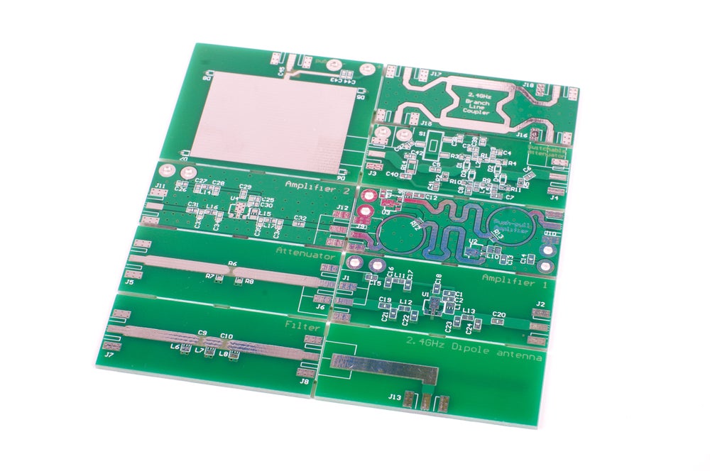
Most 5G radio channels, from sub-6 GHz small cells to phased-array mmWave modules, rely on four core functions in their transmit and receive paths: power amplification (PA), low-noise amplification (LNA), RF switching, and bandpass filtering. How those functions are packaged varies widely. Some designs use discrete components, while others integrate them into front-end modules (FEMs), beamformer ICs, duplexers, diplexers, or antenna-switch modules, and some add circulators or tuners.
5G RF front-end module design means matching each part’s electrical limits to the rest of the chain rather than optimizing for any single datasheet spec. A PA with too little linearity margin fails spectral mask testing, and any loss ahead of the LNA, such as a lossy filter or switch, adds directly to the receiver’s noise figure.
This article covers selection criteria for these four functions, whether you source them as discrete parts or as part of an integrated module, along with how package type affects thermal dissipation and the layout and sourcing decisions to follow.
The Sub-6 GHz and mmWave Front-End Signal Chain
5G New Radio (NR) splits into two frequency ranges (FR), defined in 3GPP TS 38.104, and each pushes component selection differently.
- FR1 (sub-6 GHz): roughly 410 MHz to 7.125 GHz as defined in 3GPP Release 17, including bands n41 (2.496 to 2.69 GHz), n77 (3.3 to 4.2 GHz), n78 (3.3 to 3.8 GHz), and n79 (4.4 to 5.0 GHz).
- FR2 (mmWave): FR2-1 spans 24.25 to 52.6 GHz, and Release 17 extended NR operation to 71 GHz (FR2-2). Common FR2-1 bands include n257, n258, n260, and n261, covering roughly 24 to 40 GHz.
Sub-6 GHz front-ends often use discrete blocks with room for individual matching networks, though integrated switch-LNA modules are common on the receive side. mmWave front-ends push further toward integrated GaN or SiGe modules combining the PA, LNA, and switch in one part, since mmWave boards lack room for separate matching per stage. In practice, the level of integration is a design choice, so the criteria below apply whether a function is a standalone component or a single block within a module.
Selecting Power Amplifiers for 5G RF Front-End Module Design
PA selection starts with three interlocking specs:
- P1dB (1 dB compression point): the output power where gain has dropped 1 dB from its small-signal value. Operating too close to P1dB compresses the waveform and raises error vector magnitude (EVM).
- Linearity: measured as adjacent channel power ratio (ACPR) and EVM under a realistic modulated waveform. Qorvo’s QPF4001 GaN mmWave FEM lists 35 dBc ACPR and 3% EVM at 23 dBm average output, tested with a 400 MHz OFDM, 256QAM signal.
- Efficiency (PAE): power-added efficiency sets thermal load and supply budget, and trades against linearity headroom.
Package selection follows from the PA’s electrical and thermal requirements. For example, sub-6 GHz small cell and massive MIMO PAs commonly ship in compact leadless packages such as QFN, while higher-power macro base station PAs often move to larger air-cavity or overmolded flange packages. By contrast, mmWave PAs often use air-cavity laminate packages with embedded copper heat slugs because tight beamforming element spacing can limit the use of conventional heatsinks.
Choosing Low-Noise Amplifiers for Receive Sensitivity
In the receive chain, the first LNA sets most of the noise figure, since each later stage contributes proportionally less noise. Loss ahead of the LNA, such as a filter or switch, adds to the figure dB for dB. A sub-6 GHz LNA in a switch-LNA module can reach a noise figure of 1.0 to 1.25 dB at 3.5 to 3.6 GHz, based on Qorvo’s QPB9378 and QPB9380 modules.
mmWave receive paths run noisier. Qorvo’s QPF4001 lists a typical noise figure of 3.5 dB for its LNA-plus-switch receive path at 26 to 30 GHz, as device limits and higher substrate and package loss both push the figure up.
Designers should also check third-order intercept point (IP3), which sets headroom against adjacent-channel blockers, and gain flatness across the band.
RF Switches and Filters: Insertion Loss and Isolation
RF Switch Selection: Insertion Loss vs. Isolation
Antenna and transmit/receive (TR) switches trade insertion loss against isolation and power handling. Three points shape the choice:
- Insertion loss at high power: Qorvo’s QPB9378 switch-LNA module integrates a high-power SPDT switch, with 0.5 dB transmit-mode insertion loss and 20 W average power handling, for 5G time-division duplex (TDD) base stations.
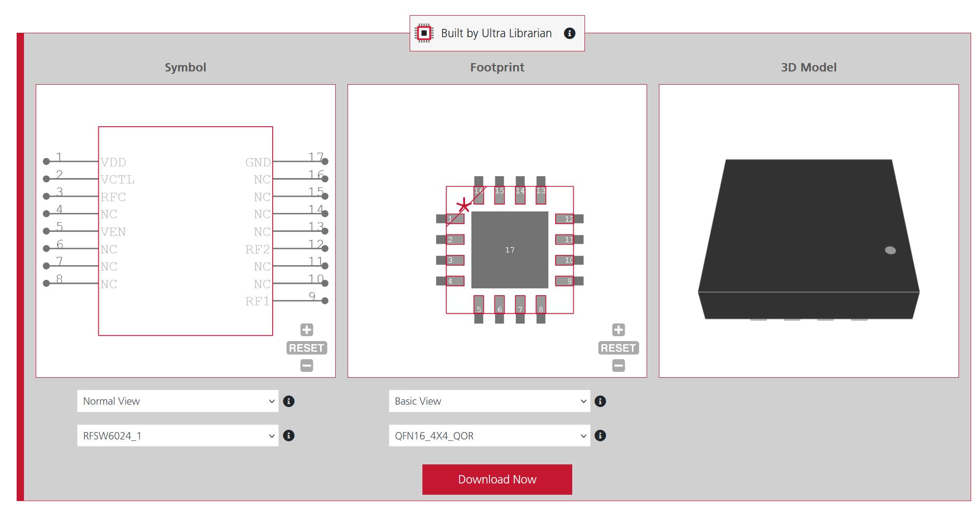
- Package and footprint: A standalone switch such as the Qorvo RFSW6024 handles about 4 W (36 dBm) with 0.55 to 1.1 dB insertion loss across 5 MHz to 6 GHz in a 4 × 4 mm QFN package, so accurate pad geometry and exposed-pad placement matter during footprint selection.
- mmWave integration: In mmWave arrays, the TR switch is often integrated with the PA and LNA, since a separate discrete switch would add interconnect loss between stages.
Filter Selection by Frequency Band
Filter choice depends on frequency:
- SAW limits: Standard surface acoustic wave (SAW) filters lose selectivity and show more temperature drift above roughly 2 GHz, though temperature-compensated designs extend the usable range.
- BAW in sub-6 GHz: Bulk acoustic wave (BAW) filters take over in the n41, n77, and n78 bands. Qorvo’s QPQ3550 BAW filter, for example, lists a maximum insertion loss below 2 dB across the 3.55 to 3.7 GHz band.
- Power handling: BAW devices can also tolerate higher power levels than many SAW alternatives, an important consideration for filters in the transmit path.
Package Selection and Thermal Dissipation
In 5G RF front-end module design, package choice drives thermal performance as much as board space. Because parts in a dense front-end module sit within millimeters of each other, the weakest thermal path sets the layout’s ceiling.
Package and Thermal Comparison for 5G RF Chips
| Package Type | Thermal Path | Typical Use | Trade-off |
| QFN (leadless) | Exposed pad soldered to ground | Sub-6 GHz small cell PAs, switch-LNA modules | Low cost with solid thermal performance; needs thermal vias under the exposed pad |
| WLCSP | Heat moves through solder bumps into the board | LNAs, switches, low-power ICs | Smallest footprint; weakest thermal path |
| Air-cavity laminate | Embedded copper heat slug under the die | mmWave PAs in phased arrays | Handles concentrated heat; higher cost |
Layout Guidance for Front-End Components
Component selection only pays off if the layout preserves what the datasheet promises.
- Ground every RF pad directly. Every ground pin, including source pins on FET-based parts, needs a dedicated via within about 10 mils of the pad edge. Give each shunt matching element its own ground via as well. A shared, daisy-chained via adds inductance, which can show up as gain loss, instability, or lost isolation.
- Stitch the ground fill around every RF trace. Keep stitching-via spacing under one-twentieth of the guided wavelength, which is shorter than the free-space wavelength on laminate. At 28 GHz, with an effective dielectric constant near 3, the limit works out to roughly 0.3 mm between vias. At 3.5 GHz, it relaxes to roughly 2.5 mm.
- Keep matching networks close to the IC pins. Hold the trace to the first matching element as short as the footprint allows. Extra length adds phase shift, which can raise standing wave ratio (SWR) and can detune the match at mmWave frequencies.
Sourcing Challenges for RF Front-End Components
RF front-end parts carry sourcing risk a general-purpose IC does not. For instance, many PAs and switches run on GaAs or GaN processes through a handful of compound-semiconductor foundries, so a single-sourced part becomes a critical-path risk once the foundry enters allocation.
Likewise, acoustic-wave filters carry the same exposure, often qualified from one supplier’s fab with no second source. Meanwhile, RF GaN-on-SiC capacity has stayed tight, with vendors prioritizing defense and space contracts, so teams should qualify alternates before a shortage forces the issue.
Sourcing Verified CAD Data for 5G Front-End Modules
Component selection only gets a design halfway there. The fine-pitch QFN and WLCSP packages common in 5G RF front-end module design are notoriously difficult to hand-draw accurately. A footprint off by a fraction of a millimeter on a 0.4 mm pitch part can cause solder bridging, opens, or a mismatched thermal pad at assembly.
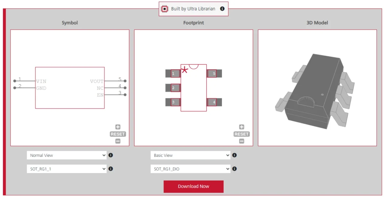
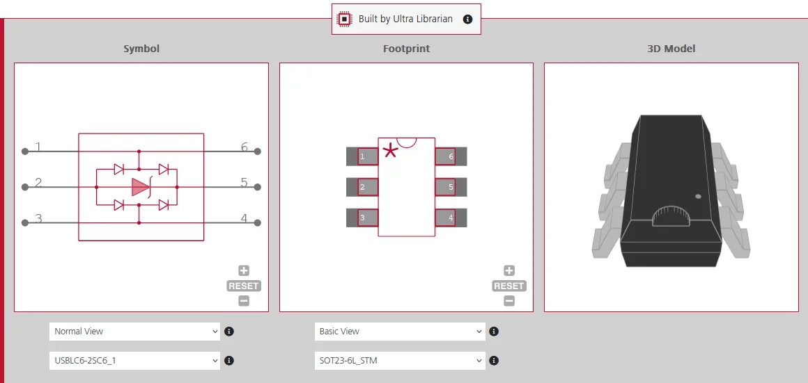
Ultra Librarian provides vendor-verified symbols, footprints, and 3D/STEP models for PAs, LNAs, switches, and filters, compatible with popular ECAD applications and sourced from worldwide distributors, so pad geometry matches the manufacturer’s specification the first time.
Working with Ultra Librarian sets your team up for success, ensuring streamlined and error-free 5G RF front-end module design, production, and sourcing. Register today for free.

 If you’re looking for any of our component footprints or models, we have readily available and free options for you and your design team. Search our library for the solution you’ve been looking for.