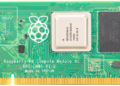
With newer products becoming more complex and requiring strict mechanical constraints, your next device will need to feel the skillful touch of a CAM engineer. MCAD programs for PCB design can be used to carefully design a sleek enclosure around your 3D electronic component models. You need to be sure your enclosure fits around your components before you send your board and enclosure off for production.
PCB design in 2D is still important and forms the foundation for a new device. However, there is some critical information you can’t see in 2D and you’ll need to use an MCAD program to see all aspects of your layout. Before you bring your new design into an MCAD program, you’ll need to find accurate 3D electronic component models for your board. These will be used to create a 3D model for your finished board, which can then be imported into your MCAD software.
What to Watch for in ECAD/MCAD Co-design
You won’t need to layout your entire board in 3D. Your layout will begin in 2D, but there are some important points to check in a 3D layout, either using PCB design software or with an MCAD application. When you have access to a verified set of 3D electronic component models, you can complete the important tasks below, which will reduce your design time and help you create higher-quality products.
Arrange Components First, Then Route Traces
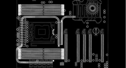
Multiboard projects, products with curved enclosures, and any board with bulky components will have tight mechanical clearances, and clearances need to be checked in 3D. Before you start routing your board, you’ll need to complete an initial component arrangement and view your board in 3D. As you’re completing the tasks listed below, you may find you need to rearrange components or swap out a component.
You should complete these important 3D design tasks before you route your traces between components. Most PCB design applications will not drag traces as you move a component. In other words, if you move a component, you’ll need to reroute the connecting traces to the new location. You can save yourself time rerouting components if you check your 3D component placement first, rather than waiting until you’ve finished your routing.
Measure Component Clearances in 3D
Multiboard projects, products with curved enclosures, and any board with bulky components carry clearance requirements to ensure manufacturability and compliance to industry standards. High voltage boards are another example of devices that carry strict component-to-component and component-to-conductor clearances in order to prevent ESD. Working in 2D with component courtyards helps you meet clearance constraints along the surface of the board, but it does not show you component clearances in 3D.
Working with your board in 3D can help you determine whether components will collide with the enclosure or each other. Working in 3D allows you to measure clearances that can’t be defined with courtyards and may not be visible in 2D. This is where you need to use accurate 3D electronic component models in your design software. Some of the best design software will include a 2D projection of a 3D component model in your layout, which helps expedite clearance measurements.
Simulate Folding and Translating Boards and Enclosures
Folding phones, laptops, cameras, and many other products with tight spacing constraints have made greater use of rigid-flex or fully-flex PCBs. The boards in these products are typically folded or molded to fit the device enclosure. A folded flex or rigid-flex PCB could require static or dynamic deformation, both of which require careful visualization of the bending region to ensure a design will fit its enclosure. Similarly, the enclosure may need to fold, which can pull on each end of the board and cause a collision with the flex ribbon.
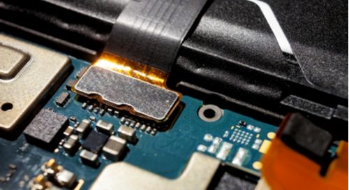
You’ll need to do more than just check lateral component clearances in these products. First, you should check that the bending region does not butt up against the side of the enclosure. Second, you should check that components do not collide as a 3D model of your board is folded. If the enclosure folds along with a flex ribbon, you need to check that the flex ribbon is long enough so it does not get pulled against the edge of the enclosure. This ability to check the clearance between the board and enclosure bending regions is critical when designing dynamic flex and rigid-flex boards.
Only Use Verified Component Models
Delegation and division of labor are what make businesses efficient and the same can be said for design teams. Not all PCB designers and layout engineers are mechanical experts and building 3D electronic component models on your own can be a time-consuming task. You’ll need to use verified 2D and 3D components as part of your design, but you shouldn’t have to build models for every component on your own.
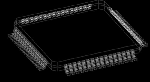
If you have CAM expertise then you can certainly build components from datasheets or you can adapt an existing 3D model for a new component. For the rest of us, you’ll need to find a source of 3D electronic component models that are complete and accurate. Distributors typically only release models for the most popular components (e.g., passives and ICs in standardized packages), leaving you to build models on your own, find them on a forum, or find them from the manufacturer.
Get the 3D Component Models You Need for Your Next PCB
When you need to find verified 3D electronic component models for your PCB, you should use a free parts aggregator service like Ultra Librarian. You’ll have immediate access to a range of verified component models supplied by manufacturers and created by CAM experts. These verified components include accurate 2D footprint information and 3D models in common vendor-specific and neutral file formats. These models can be immediately imported into popular ECAD applications and compiled into your design libraries. You’ll also have access to real-time sourcing information from worldwide distributors.
Footprint and 3D electronic component model creation takes dedicated resources and time, but Ultra Librarian helps streamline these processes. Working with Ultra Librarian will set up your team for success and ensure your finished product matches your design. Register today for free.