
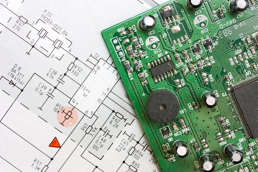
Producing circuit boards or PCBAs is a complex process that includes three stages: 1) design, 2) build, and 3) test. The first level of development for new boards is prototyping, which often requires several iterative design⇒build⇒test or DBT cycles that end with a production quality design.
The process is the same during this activity, but the board design undergoes continuous change. Sometimes, converting your schematic to a PCB design layout is required for the design stage itself. And sometimes, it may not be.
Do You Really Need a Schematic?
Sometimes, it is more informative to answer a broad question by posing and answering a set of more specific questions, as below.
- What is a PCB schematic?
A PCB schematic is a graphical representation of the components and their interconnectivity for an electrical circuit design.
- What does a PCB schematic contain?
A schematic includes symbols and labels for all necessary elements to illustrate the functionality of the circuit design. This consists of all passive and active components, reference indicators, connectors, nets, ground connections, nodes, and/or terminals.
- How is a PCB schematic used?
Schematics can be thought of as canvases for creating electrical circuit designs. Here, the design is created, reviewed, and evaluated to ensure that connectivity rules are adhered to before converting the schematic to a PCB design layout that will be manufactured.
As the answers above indicate, the schematic is typically the starting point for a new electrical circuit design. In many cases, the schematic is drawn as a template for the board’s layout.
PCBA designs are so simple that a schematic may not be necessary. For example, antenna sub-circuits, such as shown below.
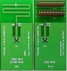
Antenna subcircuit PCBAs. from Texas Instruments.
However, the complexity of most board designs necessitates a schematic being created first to verify electrical functionality and save time on the PCB layout design.
Designing Your Board Layout
Believe it or not, there was a time when schematics and PCB layouts were drawn by hand, and those with these skills were highly sought after. Today, we have ECAD tools that greatly simplify the creation of these PCB diagrams. And converting from your schematic to PCB design layout is an auto concatenation process performed by the software. First, however, you will need to complete the following steps to prepare your design to be sent off for manufacturing.
PCB Layout Steps
Step #1: Choose a board size
Most ECAD tools include default board sizes with area and thicknesses from which you can choose. It is recommended that you check with your CM before selecting, as some board sizes may result in excessive material waste that will run up manufacturing costs.
Step #2: Create the stackup
After choosing board dimensions, you need to define the board materials, number, and types of layers.
Step #3: Arrange your components
The next step is to place the components on the board. It is important that spacing and clearance rules are followed to make sure your board can be built.
Step #4: Route the traces
Trace routing is probably the most challenging PCB layout task, especially for multilayer boards with a large number of vias–plated through holes (PTHs) that carry signals vertically to and from internal signal and ground planes. Proper spacing and clearance must also be followed when routing traces.
Step #5: Check for errors
Before sending your PCB design off to be built, you need to check the layout for errors. This includes performing a DRC analysis, which contains whether your design conforms to the design rules and constraints that were set up. These rules should be set up according to your CM’s DFM guidelines to ensure manufacturability.
The above list is not exhaustive; however, it does include the significant steps necessary to create your PCB design layout. Designing PCBAs is not a simple process. The level of difficulty and time involved to arrive at a manufacturable design will depend on the ECAD tool you use for converting your schematic to PCB design layout.
Tools for Converting Your Schematic to PCB Design
Due to the wide range of applications for electronics and circuit boards, it should not be surprising that many PCBA design packages are available. However, the range of functionality and capabilities can vary significantly among circuit board design software programs. Therefore, before opting to use any ECAD program, you should review the program’s capabilities. Some critical issues to consider that can simplify your design and save time are:
Useful PCBA Capabilities
- Component library
Creating schematic symbols and landing patterns for your PCB layout can be challenging. If your ECAD tool does not have an extensive component library, you should use an online component library to avoid manually generating component libraries.
- Netlist verification
One of the most important capabilities for schematic creation is netlist verification, which checks to make sure all wiring is connected and there are no shorts, opens, and/or floating nodes.
- Auto component placement
Another useful function is automatic component placement, which attempts to lay out the board based on component type. The effectiveness of these functions varies across tools; however, it usually provides a good starting point and does adhere to spacing and clearance rules.
- Autorouting
Autorouting is a bit more helpful than placing components, especially when many vias are involved. However, you will likely need to make changes, especially to institute good signal integrity design practices.
- Bilateral concatenation between schematic and PCB layout
All PCB design software has unilateral–schematic to PCB layout–concatenation. However, more advanced tools are capable of updating the schematic based on changes made to the layout.
Having the capabilities above will go a long way in helping your development process, specifically in simplifying the design process; including converting from your schematic to PCB design layout.
If you’re looking for CAD models for common components or useful tips; such as the best way for converting your schematic to PCB design, Ultra Librarian helps by compiling all your sourcing and CAD information in one place. Working with Ultra Librarian sets up your team for success to ensure streamlined and error-free design, production, and sourcing. Register today for free.


")