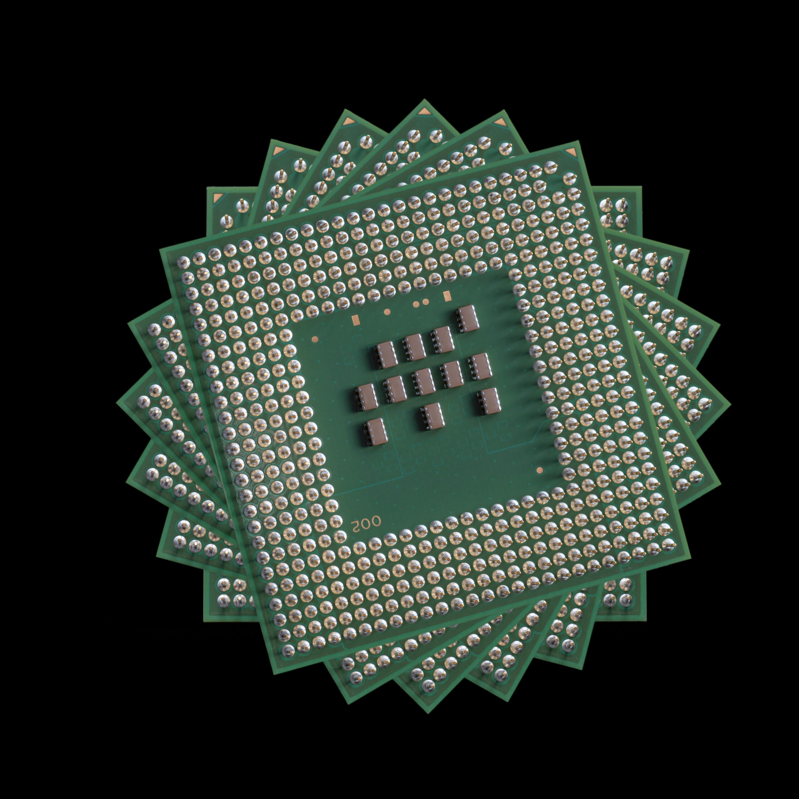
Accurate BGA footprint guidelines are critical to ensure the performance of priority components like microprocessor units (MPUs).
BGA footprint guidelines are critical design rules that determine assembly success, signal integrity quality, and manufacturing yield for ball grid array components. Proper BGA footprint design requires precise ball pattern matching, accurate datasheet package interpretation, and adherence to standards, like IPC-7351 Generic Requirements for Surface Mount Design and Land Pattern Standard, that ensure first-time-right manufacturing. This comprehensive guide covers essential BGA footprint design principles, from basic ball pattern considerations through advanced thermal and electrical requirements.
Important BGA Footprint Guidelines
Different BGA package types require specific footprint approaches based on their construction, thermal characteristics, and intended applications, as shown in the table below.
| BGA Footprint Guidelines Based on Package Type | ||||
| BGA Type | Ball Pitch | Pad Size | Solder Mask Opening | Typical Applications |
| PBGA (Plastic) | 1.27mm | 0.6mm (NSMD) | 0.65mm | Processors, FPGAs |
| CBGA (Ceramic) | 1.27mm | 0.5mm (SMD) | 0.55mm | High-reliability systems |
| TBGA (Tape) | 0.8mm | 0.4mm (NSMD) | 0.45mm | Mobile devices, compact designs |
| Fine-pitch BGA | 0.5mm | 0.25mm (NSMD) | 0.3mm | High-density applications |
| CSP (Chip Scale) | 0.4mm | 0.2mm (NSMD) | 0.25mm | Ultra-compact designs |
| μBGA (Micro) | 0.3mm | 0.15mm (NSMD) | 0.2mm | Wearable devices |
NOTE: The guidelines above are general recommendations, and you should always defer to manufacturer specifications for specific components whenever there is disagreement.
Impact of BGA Packages on PCB Manufacturing
Components that utilize BGA connections are almost exclusively high-performance devices like microprocessors and field programmable gate arrays (FPGAs), and are often deployed in products where optimizing space is a priority. Variations in materials used and construction are major factors that define footprint characteristics and, consequently, PCB manufacturing processes. For example:
Plastic Ball Grid Arrays (PBGAs) feature plastic substrates with solder balls attached directly to package pads. These components typically use a 1.27mm ball pitch and require non-solder mask defined (NSMD) pads for optimal solder joint formation.
Ceramic Ball Grid Arrays (CBGAs) use ceramic substrates that provide superior thermal performance but require different pad geometries. The ceramic construction allows for smaller pad sizes while maintaining joint reliability.
Fine-pitch BGAs with 0.8mm or smaller ball pitch demand a precision footprint design with tight tolerances. These components often require advanced PCB fabrication capabilities and careful solder paste stencil design.
When creating BGA footprints, it is essential to know how package type and features impact design choices. The most important of these are listed below, along with how your board build may be affected.
| BGA Construction Impact on PCB Manufacturing | |||
| Package Feature | Footprint Requirement | Design Impact | Assembly Consideration |
| Solder ball composition | Pad finish compatibility | Surface finish selection | Reflow profile optimization |
| Package warpage | Pad size adjustment | Thermal expansion matching | Assembly yield impact |
| Ball coplanarity | Pad tolerance specification | Manufacturing variation | Joint reliability |
| Substrate thickness | Standoff height planning | Component clearance | Rework accessibility |
BGAs are advantageous for connecting high-pin-count devices in compact areas. This allows for greater density on circuit boards, which in turn delivers better functionality and capabilities in smaller products. However, it is necessary to understand and follow good BGA footprint guidelines that maximize the benefits of these devices to achieve efficient design and reliable board builds.
PCB Design Optimization with BGA Footprint
Following footprint best practices is critical for successful PCB design. This way, you can consider and apply specific design actions that address BGA ball pattern matching, thermal management, signal integrity, and manufacturing.
Ball Pattern Matching and Pad Geometry
Accurate ball pattern matching requires precise interpretation of package drawings and adherence to IPC-7351 guidelines. The relationship between ball diameter, pad size, and solder mask opening directly impacts assembly yield and joint reliability. Some of the important considerations and design actions are:
- Choosing between Non-Solder Mask Defined (NSMD), which offers more flexibility for solder reflow, and Solder Mask Defined (SMD) pads, which restrict the pad size within the unmasked area.
- Pad size calculation:
- General Pad Size Formula: Copper pad diameter = Ball diameter × 0.8 to 0.9 Solder Mask Opening: Pad diameter + 0.05mm to 0.1mm Via-in-Pad Considerations: Via diameter ≤ 0.2mm for 0.5mm pitch BGAs
- Accurate datasheet component package Interpretation
- Package datasheets contain essential information for accurate footprint creation, and it is critical that footprints and other CAD models are accurate. However, interpreting this data correctly requires an understanding of industry conventions and measurement standards.
| Engineers using comprehensive component libraries report 78% fewer footprint errors compared to those creating custom footprints from package drawings. Ultra Librarian’s verified BGA footprints include manufacturer-approved pad geometries that eliminate guesswork from critical dimension calculations. |
Thermal Management in BGA Footprint Design
Many BGA components are high-heat generators, and managing heat distribution and dissipation is essential for reliable PCB operation. Footprint design plays a crucial role in thermal management through proper via placement and thermal pad implementation. Important guidelines for managing heat on your board are:
- Via placement: Position thermal vias within 0.5mm of high-power balls
- Via size: Use 0.2mm diameter vias for optimal thermal transfer
- Via density: 4-6 vias per cm² in thermal zones
- Fill considerations: Via filling prevents solder wicking during assembly
Thermal pad design for packages with exposed die attach pads requires careful attention to solder paste stencil design and assembly process optimization.
Signal Integrity Considerations for BGA Design
High-speed BGA components require careful attention to signal integrity through proper footprint design, layer stackup planning, and via optimization. The dense ball pattern of BGAs creates unique challenges for maintaining signal quality.
Critical signal integrity factors:
- Via stub length minimization for high-speed signals
- Differential pair routing through BGA escape patterns
- Power delivery network optimization for clean power
- Ground plane continuity around the BGA footprint area
BGA escape routing strategies:
- Dog-bone routing for fine-pitch BGAs with space constraints
- Via-in-pad routing for maximum routing density
- Blind/buried vias for complex layer transitions
| Engineers report that verified BGA footprints as delivered by Ultra Librarian reduce signal integrity issues by 65% because manufacturer-approved designs include optimized pad geometries and via recommendations based on extensive testing. |
Manufacturing Considerations and DFM Guidelines
BGA footprint design must account for manufacturing capabilities, assembly tolerances, and inspection requirements. Design for manufacturability (DFM) principles help ensure high assembly yields and reliable production. Key manufacturing factors to consider are:
- PCB fabrication tolerances affecting pad registration
- Solder paste stencil design for optimal paste volume
- Component placement accuracy requirements
- Inspection and test access for quality verification
- Reflow profile optimization for BGA solder joint formation
- Warpage control during thermal cycling
- Rework accessibility for component replacement
PCB Design Optimization with BGA
By following essential BGA footprint guidelines, as discussed in this article, you can reap the benefits of these devices operationally. Additionally, you can improve your design and development process speed and efficiency. For example, the following design implementations may increase board yield, which will lower manufacturing costs and raise design and development ROI.
| PCB Yield with BGA Optimization | |||
| Design Factor | Standard Practice | Optimized Approach | Yield Improvement |
| Pad size tolerance | ±0.05mm | ±0.025mm | 12% increase |
| Solder mask registration | ±0.075mm | ±0.05mm | 8% increase |
| Paste stencil thickness | 0.125mm | Optimized per pitch | 15% increase |
| Component placement | ±0.1mm | ±0.05mm | 18% increase |
BGAs are special pin connection architectures that require following specific guidelines to ensure manufacturability, minimize thermal issues, and achieve good signal integrity. The key lies in the accuracy of the footprints, which require precision in their creation. The best option to ensure your footprints adhere to industry standards and accurately represent the manufacturer’s intent is to rely on Ultra Librarian, the industry leader in creating CAD models.
If you’re looking for CAD models for common components or design information, such as the best BGA footprint guidelines, Ultra Librarian helps by compiling all your sourcing and CAD information in one place.
Working with Ultra Librarian sets up your team for success to ensure streamlined and error-free design, production, and sourcing. Register today for free.