
The electronics industry is highly standardized, and it has led to massive levels of interoperability, something that is not seen to the same depth in other areas of technology. Standards are applied at the product level, board level, chip level, and protocol level, all of which create constraints for board designers. Among the specifications that the industry has standardized, the Joint Electron Device Engineering Council (JEDEC) standard has helped drive interoperability in one area of computing architecture: memories.
The JEDEC group’s origins stretch back to 1944, and its footprint has steadily expanded over time to cover multiple types of memories and device specifications. As a top-tier standards organization, the JEDEC group maintains relationships with other vital electronics standards organizations like IPC and SMTA. Therefore, when searching for interface and signaling standards on memory devices, a designer’s first stop will be a JEDEC standards document. Keep reading to see a summary of what is covered in the JEDEC standards.
JEDEC Standards Overview
The JEDEC group consists of 50 committees and subcommittees composed of volunteers from hundreds of member companies. The standards organization was known initially as JETEC (Joint Electron Tube Engineering Council) and existed primarily to specify part numbering systems. Today, the group is focused on developing standards on microelectronic technologies and is responsible for developing some of the industry’s most broadly accepted standards. However, the group is probably best known for creating DDR, SDRAM, and other memory devices standards.
Over time, the organization expanded its footprint to address issues related to outsourced manufacturing and the growing commercialization of semiconductors and PCs in the 1980s. As a result, JEDEC continues to publish new standards, ranging from advanced memory devices to recently commercialized devices like wide bandgap semiconductors (GaN and SiC devices). Unlike some other standards organizations, all JEDEC standards are available for free and downloaded from the group’s website.
New memory technologies have been introduced; new JEDEC standards have been published and overhauled to sync with new technologies. A more recent publication addresses the need to prevent the proliferation of counterfeit electronics, which specifies requirements on handling, vendor/distributor vetting, chain of custody, customer return processes, and much more. A recent customer notification standard also provides procedures for informing customers of changes to semiconductor products or processes.
JEDEC Memory Standards
Memory standard sets are the best-known device standards published by JEDEC. These standards include electrical performance and product testing requirements. The list of standards falls into three main categories:
Main Memory (RAM)
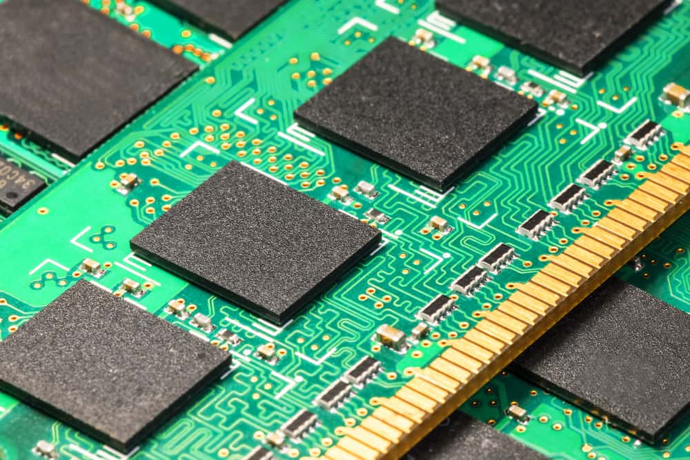
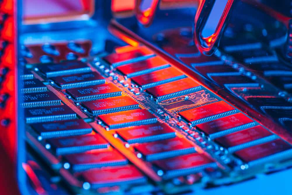
The JEDEC Main Memory standard provides performance standards for synchronous DRAM (SDRAM) and double data rate SDRAM (DDR SDRAM), the latter of which includes DDR3, DDR4, and DDR5. The DDR standards are also specified in GPU versions, with the newest and most advanced being GDDR5.
Mobile Memory
JEDEC Mobile Memory standards focus on memory devices used in mobile devices, where the focus is primarily on specifying power consumption and density. These standards include the low-power DDR (LPDDR) standard, which specifies products for mobile products but with comparable performance to desktop products. Additional Wide I/O standards are used to specify high-bandwidth memory performance requirements.
Flash Memory
One of the most common and easy-to-use memory standards is the JEDEC Flash memory standard. Current focus areas include solid-state drives (SSDs), embedded MultiMediaCard (eMMC), and Universal Flash Storage. These products are used in everything from USB drives to small consumer devices and IoT products.
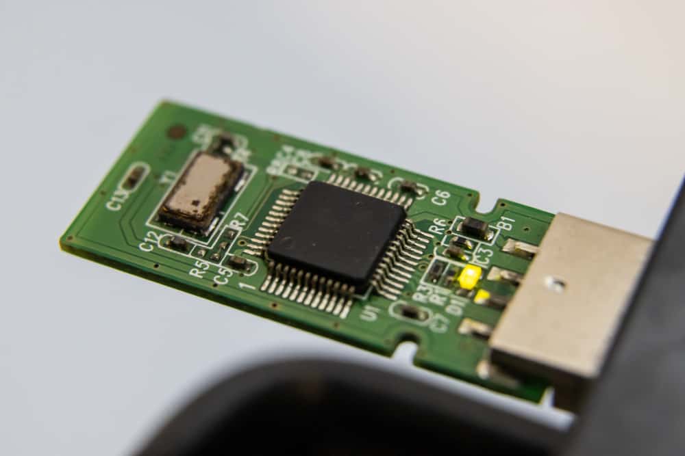
USB drives incorporate high-capacity Flash memory chips.
JEDEC Package Standards
In addition to memory standards, JEDEC specifies package outlines for common semiconductors, including many well-known packages found on discrete components. These component package naming conventions are structured using an alphanumeric code. Common package code prefixes are:
- Diode Outline (DO)
- Microelectronic Outline (MO)
- Microelectronic Standards (MS)
- Transistor Outline (TO)
- Fine-pitch Ball Grid Array (FBGA)
This standardization aids design reuse and obsolescence management and aids in locating components for designs. The FBGA package is commonly used for memory components like DRAMs; an example for a 4 GB DDR3 RAM component is shown below.
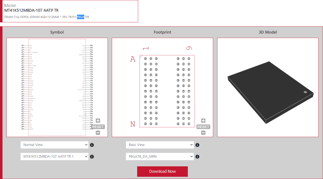
Example symbol, footprint, and 3D model of the package for MT41K512M8DA-107 from Micron.
Note that JEDEC does not necessarily specify component land patterns. Component manufacturers may provide the reference footprints that they have qualified in standard wave/reflow solder processes or use an IPC standardized land pattern. Note that the IPC has its own naming conventions for packages/footprints that differ from JEDEC, so don’t be surprised if you see alternative package/land pattern names in a datasheet.
When you need to find footprints, datasheets, and application notes for components that conform to JEDEC standards, you can quickly find the components you need with the parts search features in Ultra Librarian. The Ultra Librarian platform gives you access to PCB footprints, technical data, and ECAD/MCAD models alongside sourcing information to help you stay ahead of supply chain volatility. All ECAD data you’ll find on Ultra Librarian is compatible with popular ECAD applications and is verified by component manufacturers to help streamline your designing process.
Working with Ultra Librarian sets up your team for success to ensure streamlined and error-free design, production, and sourcing. Register today for free.


")