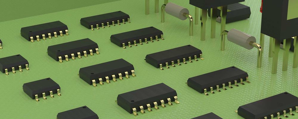
3D view of circuit board
It is common to approach PCB layout from a two-dimensional perspective. This follows from the fact that layout design typically begins with conversion from a schematic, where creating an accurate netlist free of connection errors is the primary concern. However, multilayer PCBA design necessitates that a 3D board view is adopted.
The ability to view an electronic circuit board in 3D allows designers to inspect and correct errors that could cause manufacturing delays or even redesigns. ECAD/MCAD collaborative design is also more efficient when PCB designers have 3D capability. By far, STEP file formats are the most widely used for these purposes. And integrating a STEP file viewer into your design tool box can deliver many advantages for your PCBA development.
The STEP File Format Structure
Standard for the Exchange of Product data or STEP files are vendor-neutral CAD models to promote efficient design and development. This ISO 10303 standard format was initially intended for MCAD and has the following general file format structure, as defined in ISO 10303-21.
| STEP FILE FORMAT STRUCTURE | |
| Section | Information |
| HEADER | |
| File_Description | Description
Implementation_level |
| File_Name | Name
Time_stamp Author Organization Preprocessor_version Originating_system Authorization |
| File_Schema | Schema In EXPRESS* data modeling language |
| File_Population | Governing_schema
Determination_method Governed_sections |
| Section_Language | Default language specification |
| Section_Context | Additional context specification |
| DATA | |
| Instance name | Unique instance name
Attribute value Data type mapping |
* EXPRESS is defined in ISO 10303-11.
The ability to create the STEP file format above is becoming increasingly necessary for ECAD because of the promotion of ECAD/MCAD integration to optimize the product development process for mechanical systems that include PCBAs and electronics.
Advantages of 3D File Formats for PCBA Design
The complexity of electronic circuit design today, which often includes multilayer components and stackups, places designers without 3D capabilities at a distinct disadvantage compared to other PCBA engineers. The ability to express your design in a 3D file format has a number of advantages over 2D file specifications like commonly used Gerber files. These include the following:
Benefits of 3D File Format PCBA Designs
- Improve design accuracy
The ability to view and inspect your board in 3D, enables you to make corrections to your board’s stackup during design that would otherwise require redesign after discovery during manufacturing.
- Help facilitate manufacturability
3D PCBA modeling promotes the use of digital twin technology, which is used by leading CMs to monitor board manufacturing quality and minimize process risks.
- Incorporation of mechanical designs
3D capability also improves the workflow and efficiency of ECAD and MCAD teams. The ability to work with a single file format reduces errors and reduces development time and costs.
As the above list indicates, the ability to work with CAD models and files in a format like 3D STEP can be vital for optimizing board development. Therefore, it is important to know what STEP file tools are available.
3D STEP File Viewer Tools
The most advanced PCBA design packages include the ability to import, view, and export STEP files. If your design tool does not have these capabilities, you will need to know how to use one of the 3D STEP file viewers available online. Viewing STEP files is a critical functionality for integrating this format into your design process. However, a viewer alone is not sufficient to take advantage of the benefits that 3D file formats can provide. Additionally, you need to utilize CAD libraries for your components, as well.
If you’re looking for CAD models for common components or helpful design tips about integrating the STEP file format and using a 3D STEP file viewer, Ultra Librarian helps by compiling all your sourcing and CAD information in one place. Working with Ultra Librarian sets up your team for success to ensure streamlined and error-free design, production, and sourcing. Register today for free.