
Formula E car designs are based on efficient power consumption models
Electronic designs put forth significant effort into reducing system-level noise. A noise-sensitive device (or one that is noisy itself) is liable to unintentional interactions with nearby electronics that can result in malfunction or service disruption. For this reason, devices must submit to laboratory testing to establish safe operating performance. This testing requires expensive equipment and facilities, making retesting a costly proposition; instead, design teams will want to root out noise at the source with design best practices.
However, noise comes in many forms. Some of these are inescapable, although their effect can be minimized. An amplifier that boosts signals according to the gain of the network will also amplify any associated noise. Low-noise devices are just as crucial in maintaining a strong signal–to–noise ratio (SNR) and preventing unintentional coupling to nearby conductors. An op-amp that exhibits minimal broadband and flicker noise endears to high-end audio performance (among other applications) with a low voltage spectral density, as seen in the LT1115 datasheet.
LT1115 Common Applications
Analyzing Noise in the LT1115 Datasheet
Understanding low-noise devices requires an assessment of noise sources. For any modern op-amp, consider the three primary sources of noise:
- Voltage noise exhibits a nearly constant effect with a change in resistance.
- Current noise is proportional to the impedance of the source.
- Thermal noise grows with increased source resistance like the current noise but at a different rate than the current noise. The thermal noise exhibits relatively quick growth with small increases in resistance and slower growth at higher resistance values.
Noise sources combine similarly to a vector magnitude: the square root of the sum of the component squares. Because of this, when the foremost noise source is ~3 factors (or more) greater than the next highest value, it is considered the dominant source and effectively overshadows any other contributions. Note that other noise sources exist than those listed – kTC noise, for example, physically traces to the resistor but is resistance independent. The general trend is for voltage noise to dominate at low resistances, before giving way to the thermal noise and, finally, the current noise as resistance increases. For the LT1115, source resistance should be minimal to perform optimally.
Noise is also strongly dependent on the frequency. The notable value when discussing the frequency is the corner frequency (also known as the 1/f frequency), which occurs at 250 Hz for the LT1115. Below the corner frequency, and especially below 1 Hz, noise can be magnified due to the sampling time duration. The thermal noise is generally frequency-independent – its contributions are trivial except in applications that require extreme sensitivity. Meanwhile, the current and voltage noise frequency dependency is defined by
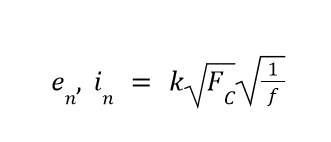
Voltage and current noise are frequency-dependent.
where k is the white voltage noise level, and FC is the corner frequency. Circuit designers can use this relationship alongside that of noise and resistance to determine the dominant source of noise.
Minimizing noise when using the LT1115 is essential. A few circuit aspects to consider:
- With a gain-bandwidth product of 40 MHz, the LT1115 is well-suited for high-gain applications. The 250 cutoff frequency allows for a maximum gain of up to 16000 (>80 dB) while leaving an appreciable buffer between the unity-gain frequencies. Conversely, suggested circuit models in the datasheet will require significant alterations to support a low-noise voltage gain. If operating at a low voltage noise, keep collector currents on input transistors to 1 mA.
- The LT1115 is unsuitable for unity-gain buffer (follower) or inverters.
- Low-impedance bypass capacitors will ensure small return loops and promote functionality when the system’s current usage spikes. Low capacitive loading and impedance feedback values prevent peaking, ringing, and oscillation.
- A good layout will include thoughtful ground plane distribution and short, direct traces to lower impedance. Power and ground traces should also widen for the same outcome. Routing over split planes should be avoided, as it causes the current loop area to expand, greatly increasing EMI to the surrounding area.
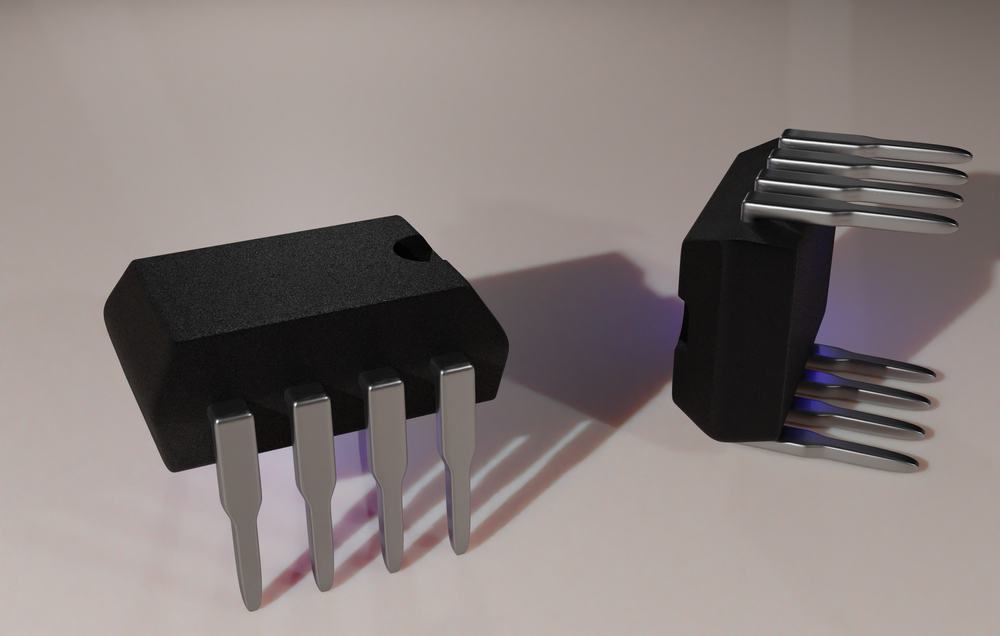
The LT1115 Pinout: Op-Amp Basics, Extra Features
Standard op-amp functionality boils down to five pins, but additional configuration options are present.
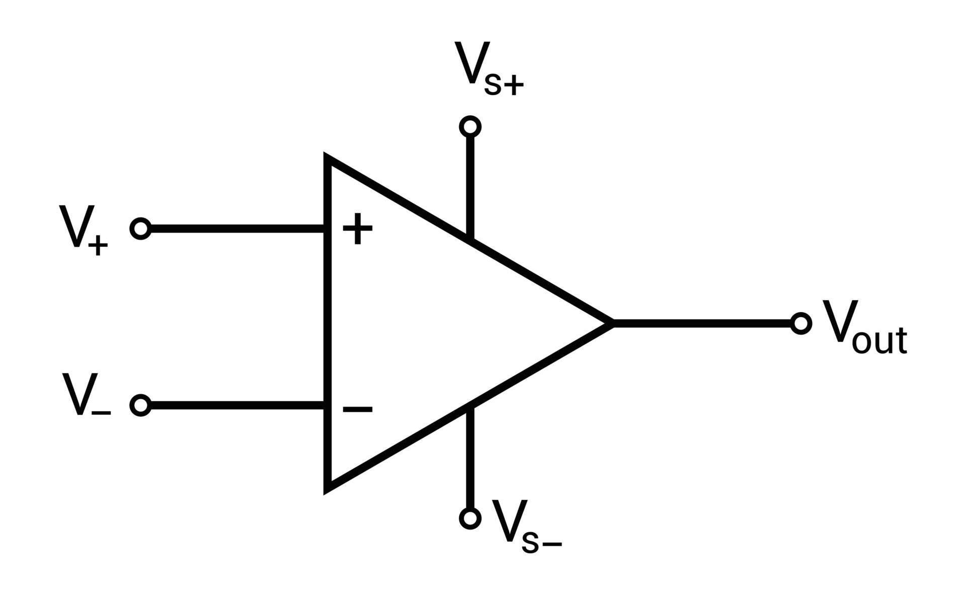
Standard op-amp functionality boils down to five pins, but additional configuration options are present.
Like all op-amps, the LT1115 follows some basic operating principles, but additional functionality is also available. The basic five pins of the op-amp – the inputs, the rails, and the output – offer the ability to pass inverting or non-inverting signals and boost them according to the open loop gain or the product of the “default” (no feedback from output to inputs) gain and the absolute difference of the positive and negative rail. The open loop gain is too large and cumbersome to be reliable outside of acting as a comparator, as even minute differences in the input voltages will cause the output to bang against the appropriate rail. In comparison, a closed loop uses a network of circuit parameters to transform the signal and purpose of the op-amp. The exact nature of the signal transformation from input to output is known as the op-amp (or op-amp network) transfer function.
However, this only accounts for five pins of the package; the remaining three active pins (the 16-pin SOIC contains 8 NC pins at the corners and those immediately adjacent) have further capability:
- Trim – Recall that two inputs connected to the same voltage line will output the corresponding rail depending on which of the inputs is slightly larger. Theoretically, the output should be zero; designers can achieve this theoretical performance by connecting a potentiometer to the trim pins and adjusting it to cancel the voltage offset at the input. Trim pins should be left floating instead of connected to ground when unused.
- Overcomp(ensation) – The overcomp pin allows the designer to increase stability and reduce bandwidth. Adjusting the overcomp pin results in a shift of the amplifier’s position on the gain-bandwidth product graph. Use of the pin also includes correcting for capacitive loads or parasitics.
Ultra Librarian Catalogs, Creates a Compendium of Components
The LT1115 datasheet gives design teams an idea of what they can expect regarding performance and application from the extremely low-noise op-amp. The most important feature when working in this range and operating conditions is a device that exhibits minimal noise due to excellent rejection rates and other fundamental device characteristics. Incorporating a low-noise op-amp starts with system-level integration; while the layout is of considerable importance, it all starts with an accurate land pattern for reliable and long-lasting solder joints. Ultra Librarian has the solution for all popular ECAD applications: a catalog of millions of component land patterns and supporting files like schematic symbols, 3D models, and SPICE simulations. An online catalog featuring parts from worldwide distributors makes finding what you’re looking for easy.
Working with Ultra Librarian sets up your team for success to ensure streamlined and error-free design, production, and sourcing. Register today for free.


")

")