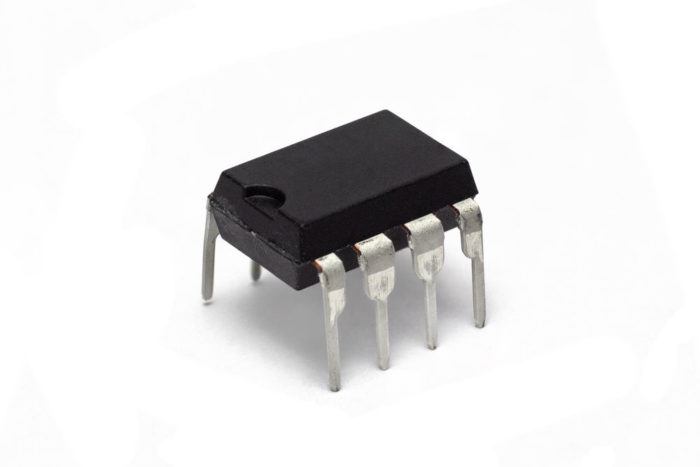
The LF356N PDIP comes in an 8-pin PDIP package for easy prototyping and through-hole assembly.
Op-amps are a key part of many circuit applications because they boost signal characteristics for further processing. Many factors go into selecting an op-amp on a pure performance basis: gain, input/output impedance, noise, susceptibility, and more. Many of these qualities come from the type of transistor used in the chip fabrication process – a CMOS op-amp differs considerably from that of the typical bipolar junction transistor (BJT). Designers may find a certain op-amp transistor type more suitable to the operation, yet almost every circuit can benefit from some of the strengths of the various types. As the LF356N datasheet demonstrates, a combination of junction field effect transistor (JFET) and BJT technology gives design teams a highly capable op-amp in a package fit for prototyping or mass production.
JFET vs. BJT op-amp characteristics
Performance Notes from the LF356N Datasheet
The LF3356N and similar chips within the family use a novel monolithic integration of JFET input op-amps alongside BJTs. Compared to the MOSFET, JFETs have a comparable gate current yet offer much better gain capabilities and lower flicker noise, making them especially suitable for low-noise applications. Additionally, JFETs offer an input impedance that falls somewhere between MOSFETs and BJTs, offering far greater input impedance than the latter implementation. In general, FET-based op-amps more closely resemble the behavior of the ideal op-amp than their BJT counterparts, precisely the input impedance and input bias current. That’s not to say BJTs’ reputation is solely that of cost-over-convenience: BJTs perform better by voltage offset bias while producing lower noise.
In this sense, the LF356N is a best-of-both-worlds approach, granting designers a unified chip that can replace bulkier and more expensive hybrid op-amp designs. As operational protection, the JFET and BJT contributions ensure large reverse breakdown voltages between the gate and source while enabling significant voltage differentials for wider applicability. However, avoid driving the voltage below the negative rail, as this can cause device failure; the same caution is not true of the positive rail, as circuits may slightly exceed (~100 mV) the positive rail without adverse performance.
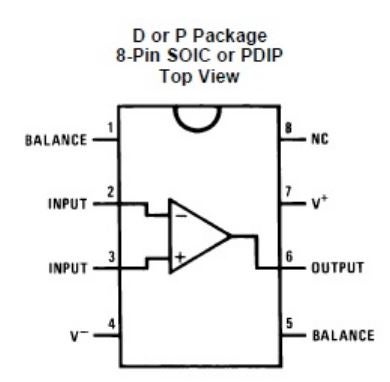
A top-down view of the LF356N package type and pinout.
The pinout is straightforward regarding op-amps: circuit designers can operate either rail at a maximum of ± 15 V (with the aforementioned “headroom” of the positive rail) and build op-amp feedback networks from pins 2, 3, and 6. The author will spare the audience the steps of basic op-amp functionality and theory, but of note is the balance function at pin 5 for the input offset voltage. The input offset voltage is a DC error (positive or negative) that occurs after powering the device and persists throughout operation, causing the output voltage to stray from zero due to differences in current draw between the two legs of the input. It is a random result of manufacturing that can differ between dies of the same wafer; the balance pin allows circuit designers to calibrate the op-amp to counter this imbalance. As JFET-type op-amps are most vulnerable to temperature drift and input offset voltage, designers will want to access this feature during prototyping.
Layout Tips for the LF356N
Circuit layout technique for the LF356N should follow general best practices: keep small capacitance decoupling capacitors close (if not directly connected) to their matching pins and generally work to shorten traces and component placement for lower impedance and loss. It’s preferable to place resistors in the feedback path closer to the input to minimize capacitance between input and ground. The LF356N layout is more exacting than a typical op-amp chip when operating with stringent leakage current requirements. However, low leakage current generally dovetails with general best layout practices and an emphasis on additional signal integrity measures to protect the circuit; these values are eminently achievable with a guard ring protecting the differential inputs of the op-amp and the terminals of any components connected to the op-amp inputs.
The guard ring successfully limits leakage current by ensuring the potential in the area surrounding the differential inputs is consistent, as current requires a voltage differential to flow. For this condition to take hold, lay designers must connect the guard ring to the inputs (or, equivalently, to ground). For prototyping purposes, designers may also want to consider using air insulation for the signals: connect the inputs/output/feedback path above the plane of the board by soldering the appropriate pins together (this will require through-hole packages for any components used, which should be trivial in a prototyping stage of development). This method has poor manufacturing scalability, yet it may be a viable solution for signal integrity for individual (or a reasonably small number) prototype boards. Lastly, consider the effects that contaminants found on the fingers – including naturally occurring salts and oils – may have on insulation/conduction of the package materials; sterile prototype handling can greatly enhance performance outcomes alongside device reliability.
Instantly Update Layout Libraries With Ultra Librarian
The LF356N datasheet has much more information regarding the nitty-gritty specifications, but designers should be familiar with the device’s operation. Once past the prototyping stage, designers will want to follow the layout guidelines outlined above for optimal board performance. Of course, board quality begins with accurate land patterns that ensure the net routing is accurate. Ultra Librarian’s popular ECAD applications include the LF356N and thousands of other Texas Instruments’ devices so design teams can accelerate electronic development without sacrificing manufacturability.
Working with Ultra Librarian sets up your team for success to ensure streamlined and error-free design, production, and sourcing. Register today for free.


")