
Collaborative PCB verification and design review before simulation or prototyping is essential for accelerating electronic systems development.
Consumers want smarter, more connected products that are reliable and affordable. Meeting this demand has spawned a more competitive landscape for companies who must address electronics systems’ accelerating complexity. A collaborative PCB design and verification environment helps minimize costs and deliver next-gen products to market faster.
PCB Design Review Challenges
Developing high-quality PCB designs efficiently presents distinct challenges:
The above challenges are even more daunting when the PCB design review and verification process needs to coordinate multiple, contributing design and engineering teams. Altair, a global technology company that provides software and cloud solutions in simulation, artificial intelligence, and high-performance computing, has successfully developed a collaborative design review and verification platform that is easily accessible by distributed teams working from different sites and regions.
Altair’s PCB Verification Solution
The Altair PCB design verification solution, Altair® PollEx™, has been adopted by global, leading companies that develop electronic systems. This new approach has been shown to reduce errors and defects that drive up manufacturing and development costs.
PollEx ensures that design for manufacturing (DFM) and design for electrical / EMC (DFE) rules and guidelines are instituted and centrally controlled, which is a critical challenge for all PCB design, manufacturing, hardware, and test engineering teams. The software’s centralized environment enables diverse groups to collaborate around and leverage new and legacy designs across facilities regardless of size or location.
Why PollEx for PCB Design Review and Verification?
- PCB verification workflows are streamlined and reliable. Learn More
- PCB design and manufacturing teams can identify potential errors earlier in the development process.
- Review and verification capabilities reduce the need for prototyping, which lowers design and manufacturing costs.
- A collaboration-friendly environment combines robust capabilities and efficient workflows with which users can improve product design processes and accelerate time-to-market.
To learn more about Altair’s solution, read the Samsung SDI case study.
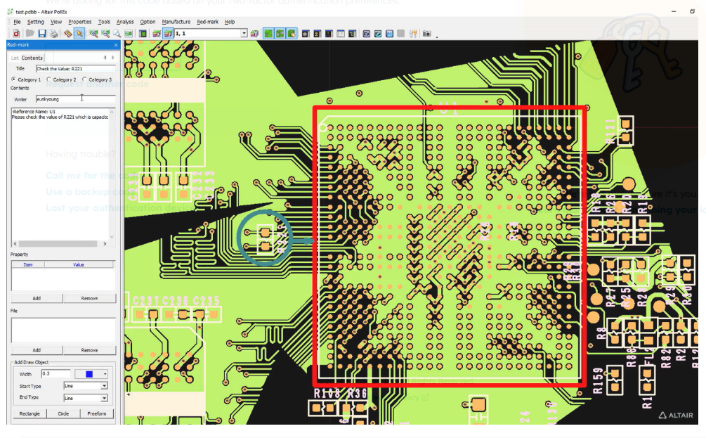
PCB design review in PollEx showing collaborators’ markup and comments on specific layers.
Efficient PCB Design Review and Verification Optimization
The gains from optimizing your PCB design process can be substantial. The best way to achieve the maximum benefit for your operations is to employ early-stage PCB design review and verification to identify and remedy errors before prototyping or mass production. Adopting a collaborative solution environment for engineers across different disciplines, sites, and regions shortens the design process.
PollEx unifies data, rules, and checks across various ECAD sources and disciplines from concept to manufacturing, eliminating design bottlenecks and errors and ensuring a smoother process for delivering high-quality boards efficiently. Discover how Samsung saves millions annually with Altair PollEx.
If you’re looking for CAD models for common components or important design information like how to use Altair tools to optimize PCB design review and verification, Ultra Librarian helps by compiling all your sourcing and CAD information in one place.


")