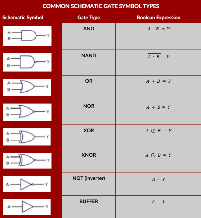
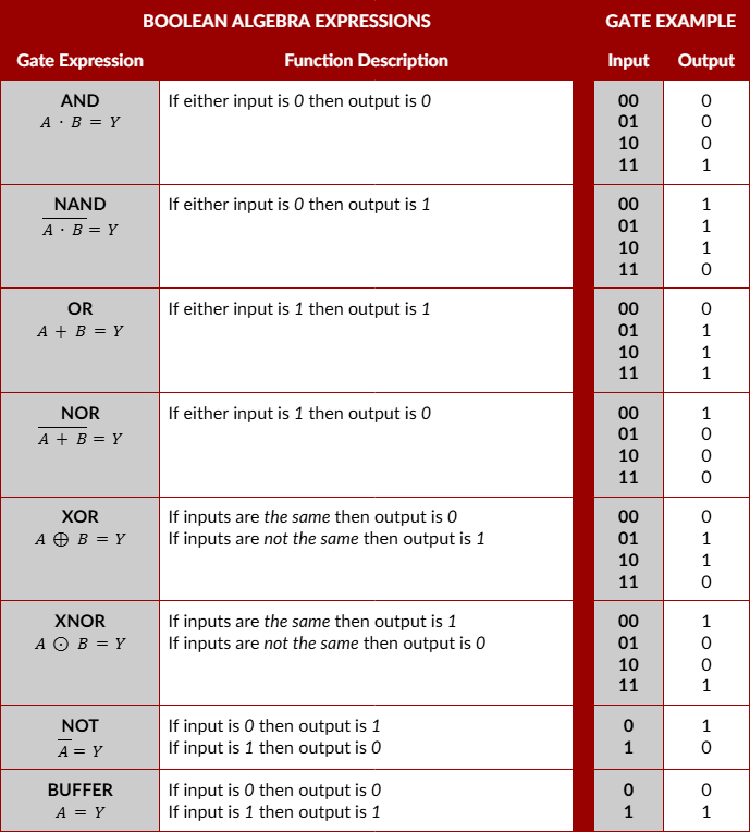
Schematic gate symbols allow engineers to visualize and efficiently design circuits that implement digital logic.
As products, appliances, and systems get smarter, the electronics that drive them become more digital. PCBs are typically classified based on construction or application. Nevertheless, circuit boards that utilize digital components are predominant for board types like embedded systems containing microprocessors (MPUs)/microcontrollers (MCUs). Designing these types of circuits effectively necessitates a good understanding of the functionality of standard digital components and the schematic gate symbols that represent the digital logic operations they perform.
Schematic Gate Symbol Types
There are many different types of digital components. Whether simple or complex, these devices contain familiar passive and active components, such as resistors, diodes, and transistors. Examples include resistor-transistor logic (RTL) and transistor-transistor logic (TTL). As digital circuits operate on a two-state system, operation is switch-like, where the device is either ON or OFF. From a signal perspective, these states are HIGH or LOW, respectively. The following common schematic gate symbols represent this functionality.

As indicated above, digital gates implement Boolean algebra functions. Consequently, it is imperative to be familiar with this base-2 mathematical system to create and design digital logic circuits effectively.
Understanding Boolean Algebra Expressions
Similar to other mathematical systems, like decimal (base-10) or octal (base-8), algebraic functionality in Boolean is illustrated by expressions that contain variables, an operator, and an equivalence symbol. The functions of the common gates defined above are presented in the table below.

Every Boolean function or operation has a complement or opposite alternative. For example, the AND gate operation indicated by a dot operator converts to a NAND gate (Not AND) operation by inverting its output. This logic symbol uses ‘⭘’ or inversion symbol on the output pin. In general, we can say the following about complementary schematic gate symbols:
How to Create a Complementary Schematic Gate Symbol
|
In the table above, we also see that AND and OR gates, NAND and NOR, and XOR and XNOR gates complement each other. This flexibility is beneficial when designing circuit gates with logic gates.
Circuit Design with Schematic Logic Symbols
Following electronic component best practices is essential for all circuit board design. For the most efficient ECAD workflow, it is critical to know and implement good schematic design guidelines. Irrespective of complexity, the schematic design process for most PCB designs follows the same paradigm. However, there are considerations unique to designing with schematic gate symbols.
Guidelines for Design with Schematic Gate Symbols
- Fully define the operational objective(s) for your digital circuit
- Truth tables are a common technique for explicitly specifying the logic operation of your circuit. These graphical elements list all 2n possible input configurations and the corresponding required output for each (unless the input/output condition is unavailable, a ‘DON’T CARE ’ situation exists, which may require special consideration, as they could be external circuit considerations).
- Use Boolean algebra to define or prove the logic for your circuit
- For reasonably simple circuits, Sum-of-Products (SOP) or Product-of-Sums (POS) can be used to specify the gates for design in an AND-OR or OR-AND configuration, respectively. State space diagrams may be necessary for more complex circuits or when timing is a critical factor.
- Convert your circuit to a single gate type
- Although single gates are available, maximally leveraging integrated circuit packages by combining multiple gates into a single device. Doing so simplifies component placement, reduces trace routing, and saves space during layout.
- Choose the gate(s) that satisfy your function and performance requirements
- When selecting components, it is vital to use an industry-leading online search tool for CAD models and to source components. Failing to do so may lead to inconsistent turnaround times, inferior or counterfeit components, or a lack of availability.
Suppose you’re looking for CAD models for standard components or important design information on schematic gate symbols. In that case, Ultra Librarian helps by compiling all your sourcing and CAD information in one place.
Working with Ultra Librarian sets up your team for success to ensure streamlined and error-free design, production, and sourcing. Register today for free.