
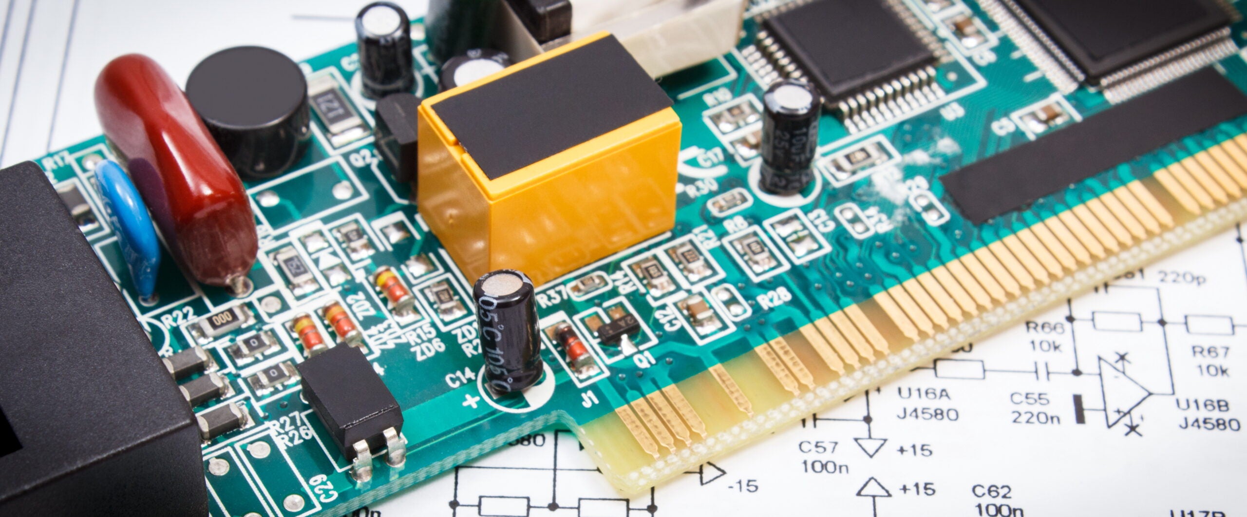
Results of a successful PCB design development process
PCB design development, which includes schematic generation and PCB layout design, is a complex engineering process that demands precision, efficiency, and access to comprehensive component libraries. Success hinges on seamless schematic capture, accurate circuit connectivity, and having the right parts data at your fingertips when design decisions matter most. The best way to avoid the many pitfalls through this process is to follow a PCB design development guide.
| PCB Design Development Workflow Overview | |||
| Design Stage | Key Activities | Common Challenges | Time Investment |
| Requirements Analysis | Define specifications and performance targets | Incomplete requirements and scope creep | 5-10% of the project |
| Schematic Capture | Component selection, circuit design, and connectivity mapping | Part availability and symbol accuracy | 20-25% of the project |
| PCB Layout Component Placement | Physical layout, thermal considerations | Space constraints and signal integrity | 15-20% of the project |
| PCB Layout Routing & Connectivity | Trace routing, via placement, and design rule checks | Layer management and impedance control | 30-35% of the project |
| Verification & Testing | DRC, electrical rule checks, and simulation | Design rule violations and timing issues | 20-25% of the project |
As you can see, the PCB design development process consists of three major stages in addition to the initial analysis: Schematic Capture, PCB Layout (component placement and routing), and Verification and Testing. However, each stage typically requires a multi-step process in its own right. For example, verification may only consist of running DRC checks. Yet any concerns would necessitate a design change and retest, which may be repeated numerous times before your design can be certified as ready for manufacturing.
Schematic Capture: The Foundation of PCB Success
Schematic capture represents the critical first step where your project objectives become a circuit concept. This stage demands access to a comprehensive electronic component database that includes accurate component symbols, comprehensive part libraries, and reliable electrical characteristics data as found in manufacturer datasheets. It is important that your schematic exhibits the following:
Key schematic capture requirements:
|
The quality of your component library directly impacts schematic accuracy. Engineers using comprehensive libraries like Ultra Librarian’s collection of over 6 million verified components report 43% faster schematic capture times compared to those building symbols from scratch.
PCB Layout Design: Ensuring Signal Integrity
Laying out your PCB is where you will design the circuit connectivity, which encompasses the electrical relationships between components and the physical trace routing that enables proper signal flow. This stage requires careful attention to component placement, impedance matching, signal integrity (SI), and power integrity (PI) for on-board and external connectors. on
Critical PCB Layout Considerations:
|
Engineers report that organized component libraries can reduce connectivity errors by upwards of 67% because verified parts include accurate pin assignments, electrical characteristics, and packaging information that prevents common routing mistakes. In addition to signal integrity and power integrity requirements, today’s smaller, denser PCBs often carry high-speed signal requirements. Some important guidelines to help you make the best PCB layout decisions for your design are listed below.
Signal Integrity Checklist:Power Distribution:
High-Speed Signals:
|
Streamline Your PCB Design Development Process
Successful PCB design development depends on accurate component data, efficient design tools, and streamlined workflows that minimize redesign and often manufacturing respin cycles. The combination of proper schematic capture techniques and comprehensive parts libraries creates a foundation for reliable, manufacturable designs.
The Ultra Librarian Advantage in PCB Development
Ultra Librarian’s comprehensive parts library transforms PCB design development by providing engineers with verified, manufacturer-approved component data that eliminates the guesswork from schematic capture and connectivity planning.
PCB Design Development Efficiency Benefits✅ Verified Component Data: Every symbol, footprint, and 3D model undergoes manufacturer verification, ensuring your schematic accurately represents the physical component you’ll receive. ✅Global Manufacturer Network: Access to parts from over 750 manufacturers means you’ll find the exact components your design requires, not just close alternatives that compromise performance. ✅ Integrated Design Flow: Seamless integration with major CAD tools eliminates the export/import friction that slows traditional design workflows. |
If you’re looking for CAD models for common components or important information on how to optimize your PCB design development process, Ultra Librarian can help by compiling all your sourcing and CAD information in one place.
Working with Ultra Librarian sets up your team for success to ensure streamlined and error-free design, production, and sourcing. Register today for free.


