IC Packaging Types: Guide

Close-up of an electronic chip in a through-hole DIP package

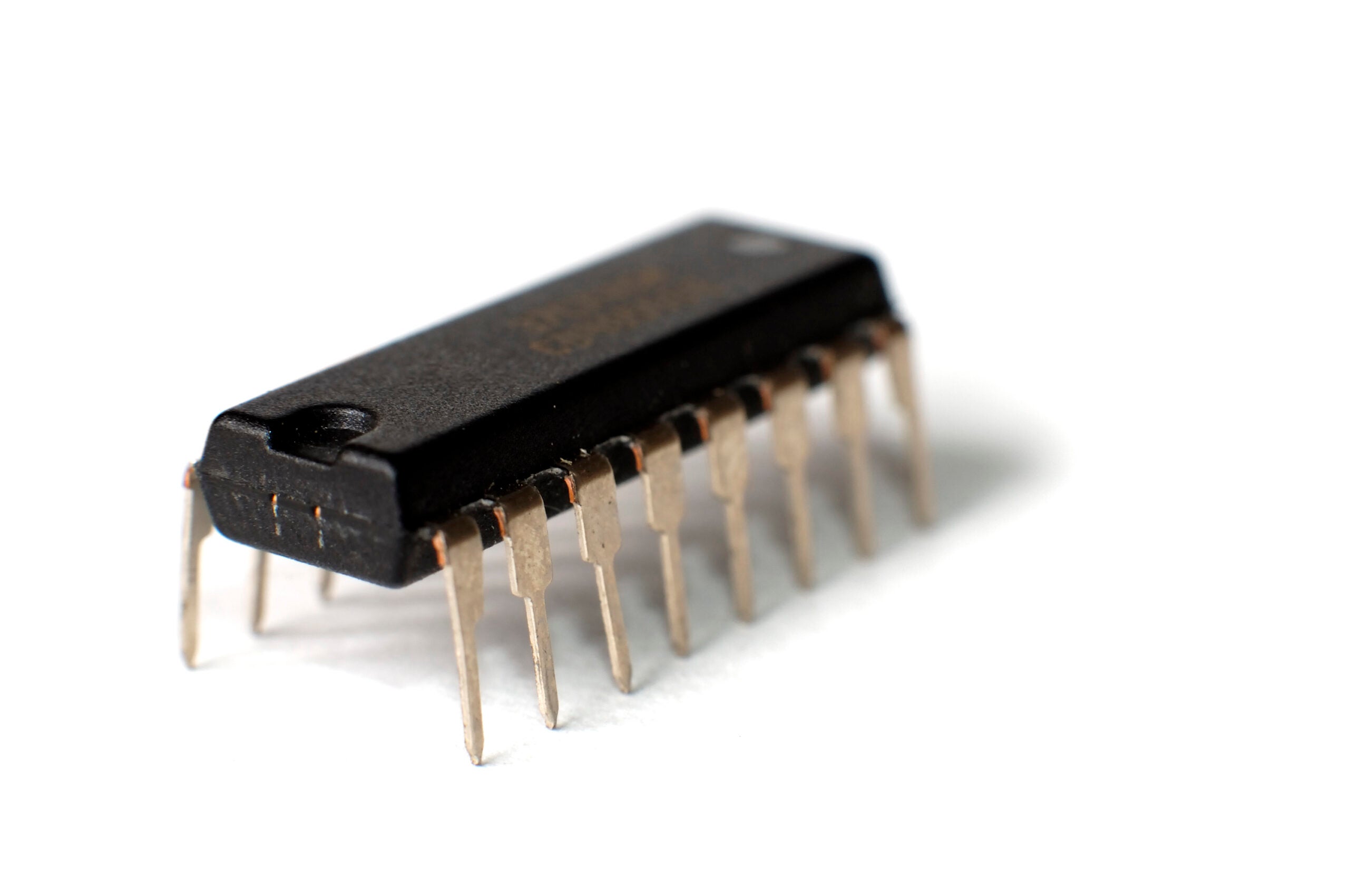
Close-up of an electronic chip in a Dual In-line Package

Integrated circuits (ICs) are the foundation of modern electronics, but their bare silicon dies cannot operate without proper protection and connectivity. IC packaging provides mechanical support, electrical connections, and thermal management. As devices become smaller and more powerful, their packaging must handle higher power densities, minimize parasitic effects, and maintain signal integrity. 

IC Packaging Types in Short

IC packaging is the final step in semiconductor manufacturing, where the silicon die is enclosed in a protective casing that provides mechanical protection, electrical connections, and thermal management. It shields the die from damage and contaminants, connects microscopic circuits to the PCB, and dissipates heat to maintain safe operation. 

IC Packaging Types Classifications

At a high level, IC packaging types can be divided into two main categories based on how they are mounted to a PCB.

  • Through-Hole Technology (THT): These packages feature leads or pins that are inserted through drilled holes in the PCB and soldered on the opposite side. THT offers a very strong mechanical connection, making it suitable for components subject to physical stress and for prototyping or hobbyist projects. The Dual In-line Package (DIP) is the most iconic example.
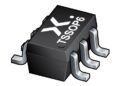
  • Surface Mount Technology (SMT): These packages are designed to be mounted directly onto metal pads on the surface of the PCB. Components using this technology are known as Surface Mount Devices (SMD). SMT allows for smaller component sizes, which in turn enable higher component densities on circuit boards. The smaller size of SMDs also enables better electrical performance at high frequencies, making it the dominant technology for modern electronics.

Dual In-line Package (DIP)

The Dual In-line Package (DIP) is a rectangular through-hole (THT) package with two parallel rows of metal pins. Once the industry standard, it remains popular due to its low cost, durability, and ease of hand soldering. However, the larger package size, limited pin count, and high lead inductance make DIPs less suitable for high-frequency or compact designs. DIPs are still common in prototypes, hobbyist projects, legacy systems, and low-frequency analog or digital circuits.

Common Surface Mount Technology IC Packaging Types

Within the SMT category, package types range from ultra-compact designs to larger, high-performance options. The table below moves from simpler, low-density IC packaging types to advanced, high-density options.

Package Type Description Benefits Drawbacks Common Applications
Small Outline Transistor (SOT) Compact SMT package for discrete components, including transistors, diodes, and voltage regulators. Many variants vary in power handling and pin count. • Very small and cost-effective
• Usually for single discrete components
• Limited current and power dissipation (in smaller variants)
• Difficult for manual soldering due to the smaller size
• Discrete transistors and diodes
• Voltage regulators
• Low-power analog and RF circuits
Small Outline Package (SOP) / Quad Flat Package (QFP) SMT packages with leads extending from two sides (SOP) or all four sides (QFP). Variants include TQFP (Thin QFP) and LQFP (Low-Profile QFP) . • Smaller footprint and higher pin count to DIP
• Good thermal performance
• More difficult to handle and solder
• Requires specialized SMT assembly equipment
• Microcontrollers
• Automotive electronics
• Consumer electronics
Ball Grid Array (BGA) SMT package with solder balls on the underside instead of leads. Enables very high pin density and compact size with different material variants. • Very high I/O density
• Excellent electrical/thermal performance due to short interconnect paths
• Hidden solder joints (requires X-ray for inspection)
• Complex and costly rework
• CPUs, GPUs, FPGAs, ASICs
• High-speed memory modules
Chip-Scale Package (CSP) Extremely compact package, nearly the same size as the silicon die (≤1.2× die size). Represents maximum miniaturization for single-die ICs. • Ultra-small, high-performance due to minimal interconnect length • Difficult inspection and rework
• Thermal management challenges due to high power density
• Mobile and wearable devices
• IoT sensors
• High-density memory

Advanced IC Packaging Types

As technologies improved,  new packaging methods that integrate multiple chips within a single package are now more commonly used. Examples include:

  • System-in-Package (SiP) & Multi-Chip Modules (MCM): These packages integrate multiple distinct ICs (like a processor, memory, and RF chip) and passive components into a single module.
  • 2.5D and 3D IC Packaging: This involves stacking dies to achieve higher density and performance. 

    • 2.5D places dies side by side on a silicon interposer for high-speed communication, commonly found in High-Bandwidth Memory (HBM). 
    • 3D ICs stack dies vertically, connected with Through-Silicon Vias (TSVs), minimizing interconnect length for ultimate performance and footprint reduction.
  • Wafer-Level Packaging (WLCSP / FOWLP): In these techniques, the packaging is applied at the wafer level before the dies are separated. 

    • Fan-Out Wafer-Level Packaging (FOWLP) is notable because it extends the routing area beyond the size of the silicon die, allowing for a higher I/O count than the die itself would normally support.

How to Choose the Right IC Package Type

Choosing the right IC package depends on a few key factors, and considering them step by step can help guide the decision.

  1. Pin Count: The first question is usually how many I/Os your design needs. If you require a large number of pins, high-density packages such as BGA or CSP are ideal. For fewer pins, simpler packages like SOT or SOP/QFP may be sufficient.
  2. Performance Requirements: High-speed or high-frequency circuits benefit from packages with low parasitic inductance and capacitance, such as BGA or CSP, which keep interconnects short.
  3. Size and Form Factor: Compact devices like wearables or mobile electronics require ultra-small packages, making CSP or Fan-Out WLP (FOWLP) attractive options. Larger boards with more space can accommodate SOP/QFP or BGA.
  4. Thermal Management: High-power components need packages with good thermal pathways, such as BGA with thermal vias or packages with exposed pads to help dissipate heat efficiently.
  5. Cost and Manufacturing: Finally, consider production capabilities and budget. Packages like SOT and SOP/QFP are easy and inexpensive to handle, whereas BGA, CSP, and FOWLP require advanced assembly and inspection, which adds to the cost.

By evaluating these factors, you can select the package that best balances electrical performance, reliability, and cost for your application.

If you’re looking for different IC packaging types, Ultra Librarian helps by compiling all your sourcing and CAD information in one place. Our platform provides verified, ready-to-use footprints, symbols, and 3D models that support all popular ECAD applications, along with sourcing information from worldwide distributors.

Working with Ultra Librarian sets up your team for success to ensure streamlined and error-free design, production, and sourcing. Register today for free.

UL-Icon.png

The Ultra Librarian Team

Ultra Librarian offers the world’s largest PCB CAD library, putting cutting-edge materials at your fingertips so you can build better products faster—all for free.

Join Our Newsletter

Subscribe to our newsletter to receive the latest news, and important updates

Name(Required)

Related Posts

If you’re looking for any of our component footprints or models, we have readily available and free options for you and your design team. Search our library for the solution you’ve been looking for.

IC Manufacturers

Working with us allows you to target the right audience for your component, provide content to nurture them along their design process, and analyze how your parts are being received and used.

How do manufacturers help shape the pcb design engineer’s journey?

Download now to discover how manufacturers support PCB design with data, tools, models and more.

Part Details

Pricing by

Free Design Resources

Ultra Librarian is the worlds largest online – and always free – PCB CAD library. Build products better, faster, and more accurately with easy access to vendor-verified symbols, footprints, and 3D models. Register today to start searching the right components for your next design.

Recommended

PHP Code Snippets Powered By : XYZScripts.com