
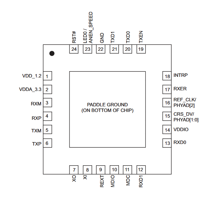
Pin Out from the KSZ8081 Datasheet
From streaming movies on a smart TV to connecting office computers to the network, the wired Ethernet connection remains a key part of reliable, high-speed data transfer. While we often see the familiar Ethernet cable, the real work of translating electrical signals into digital data happens inside the device, on a specialized chip known as an Ethernet Physical-Layer Transceiver, or Ethernet PHY. This chip acts as the bridge between the digital logic of a processor or microcontroller and the physical Ethernet cable, handling tasks such as signal encoding, decoding, clock recovery, and link detection to ensure a smooth connection.
The KSZ8081 from Microchip is one such example—a single-supply 10/100 Mbps Ethernet PHY engineered specifically for reliable, low-power network connectivity. Its compact design, low energy consumption, and reduced pin count make it an excellent fit for embedded systems, industrial control units, consumer electronics, and other connected devices that require dependable wired networking. This overview serves as a quick reference guide to the KSZ8081 datasheet, highlighting its key features, package options, and practical implementation details for design engineers.
KSZ8081 Datasheet: Key Features and Specifications
The KSZ8081 is built for efficient integration in devices that need reliable wired Ethernet, such as industrial controllers, Internet Protocol (IP) cameras, routers, and smart appliances. In an Ethernet system, the Physical Layer (PHY) chip converts digital signals from the processor into electrical signals on the cable and back again, while the Media Access Controller (MAC) manages data framing and network control.
The KSZ8081 uses a Reduced Media-Independent Interface (RMII) to connect the PHY to the MAC. RMII streamlines this link by cutting the number of required data lines in half compared to the older MII standard, reducing pin count, board space, and power consumption.
KSZ8081 Key Specifications
The chip is designed for embedded and industrial systems requiring dependable 10/100 Mbps connectivity. It offers flexible power options, built-in diagnostics, and protection features to simplify design and improve system reliability.
- Ethernet Speed: Supports 10 Mbps (10BASE-T) and 100 Mbps (100BASE-TX) operation
- Processor Interface: Reduced Media-Independent Interface (RMII) v1.2 with 50 MHz reference clock output to the Media Access Controller (MAC)
- Power Supply: Single 3.3 V operation with internal Low-Dropout Regulator (LDO) generating 1.2 V core voltage
- I/O Voltage Options: 1.8 V, 2.5 V, or 3.3 V for direct interface with different host controllers
- Low-Power Modes: Standard power-down and Energy-Detect Power-Down for reduced idle consumption
- Diagnostics: LinkMD® (Link Monitor Diagnostic) using Time-Domain Reflectometry (TDR) to detect cable faults like opens, shorts, or impedance mismatches
- Protection: ±6 kV Electrostatic Discharge (ESD) protection on Ethernet (MDI) pins
KSZ8081 Package Options
According to the KSZ8081 datasheet, the chip is available in two packages: a compact 24-pin, 4 mm × 4 mm Quad Flat No-leads (QFN) package (KSZ8081RNA) or a 32-pin, 5 mm × 5 mm QFN package (KSZ8081RNB). QFN packages are low-profile surface-mount designs with pads on the underside instead of traditional leads. Both package options are Available in Commercial (0°C to +70°C) and Industrial (-40°C to +85°C) temperature grades.
- Overall, choose the KSZ8081RNA for maximum board space savings.
- Choose the KSZ8081RNB if you require the hardware-based configuration without software intervention or prefer dedicated LED driver outputs.
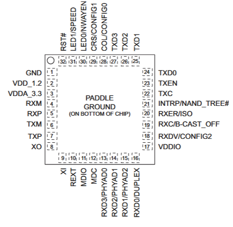
KSZ8081RNB Pin Out Diagram
Datasheet
KSZ8081 Package Differences
KSZ8081 Typical Integration and Design Considerations
In this section, we walk through a typical KSZ8081 application, using a block diagram to show how the PHY connects a processor to the network and highlighting the key design considerations that ensure reliable Ethernet performance.
The block diagram below illustrates the core signal flow. The processor’s Media Access Controller (MAC) connects to the KSZ8081 PHY via the digital RMII, and the PHY converts these signals into differential pairs (TXP/TXN, RXP/RXN) that pass through Ethernet magnetics to the RJ-45 connector. This flow illustrates how digital data from the host becomes physical Ethernet signals while maintaining signal integrity and isolation.
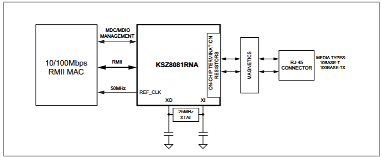
Pin Example System Block Diagram for a KSZ8081RNA chip.
Besides the signal flow, several aspects of the KSZ8081 design are especially important for integration:
- Configuration Straps: Pins such as PHYAD0, MODE0, and MODE1 set default behaviors like PHY address and auto-negotiation. Pull-up or pull-down resistors are required to avoid floating states.
- Power Supply Decoupling: All power supply pins (VDDA, VDDIO, etc.) must be decoupled with high-frequency, low-ESR 0.1µF ceramic capacitors. These capacitors must be placed as close as physically possible to their respective pins to ensure a low-impedance path and stable operation.
- RMII Reference Clock (REF_CLK): The PHY provides a 50 MHz clock to the MAC. The MAC should be configured to accept this external clock to ensure synchronized, error-free data transfers.
- MDI Termination: Cable-side center taps use high-voltage capacitors to filter common-mode noise, improve EMI performance, maintain signal integrity, and ensure safety across the isolation barrier.
When implemented carefully, these elements allow the KSZ8081 to deliver dependable, high-speed Ethernet connectivity across a wide range of embedded applications.
If you’re looking for the KSZ8081 datasheet or CAD models, Ultra Librarian helps by compiling all your sourcing and CAD information in one place. Our platform provides verified, ready-to-use footprints, symbols, and 3D models that support all popular ECAD applications, along with sourcing information from worldwide distributors.
Working with Ultra Librarian sets your team up for success, ensuring streamlined and error-free design, production, and sourcing. Register today for free.


")
