 For audio engineers and hobbyists alike, the quest for high-power amplification in a small footprint invariably leads to Class D topology. Among the controllers available, the Infineon IRS2092 stands out as a high-voltage gate driver with a self-oscillating pulse width modulator, allowing for designs ranging from 50W to 500W with remarkably low distortion.
However, the performance of a Class D amplifier is inextricably linked to its layout and component selection. This IRS2092 reference guide dissects the critical subsystems of a successful implementation, helping you navigate the challenges of switching noise, deadtime optimization, and thermal management to build a dependable amplifier.
For audio engineers and hobbyists alike, the quest for high-power amplification in a small footprint invariably leads to Class D topology. Among the controllers available, the Infineon IRS2092 stands out as a high-voltage gate driver with a self-oscillating pulse width modulator, allowing for designs ranging from 50W to 500W with remarkably low distortion.
However, the performance of a Class D amplifier is inextricably linked to its layout and component selection. This IRS2092 reference guide dissects the critical subsystems of a successful implementation, helping you navigate the challenges of switching noise, deadtime optimization, and thermal management to build a dependable amplifier.
IRS2092 Reference Guide
Unlike traditional Class AB amplifiers, which operate output transistors in their linear region (essentially acting as variable resistors), Class D amplifiers operate as switches. In a Class D topology, the output transistors are driven to be either fully ON or fully OFF. Since Power = Voltage × Current, the power dissipated as heat in the transistors is minimal in both states. This allows Class D amplifiers to achieve efficiencies of up to 90%, drastically reducing the need for bulky heat sinks and enabling high-power audio in very small packages.IRS2092S Pin Descriptions
| Pin # | Name | Function | Description |
| 1 | VAA | Floating Input Supply | Positive supply for the floating input section (typically +5V relative to GND). |
| 2 | GND | Input Return | Return (ground) reference for the floating input supply. |
| 3 | IN- | Analog Input | Inverting analog input (audio signal input). |
| 4 | COMP | PWM Output | Phase compensation / Comparator input. |
| 5 | CSD | Protection | Shutdown timing capacitor. Controls overload protection, delay, and self-reset timing. |
| 6 | VSS | Floating Input Supply | Negative supply for the floating input section (typically -5V relative to GND). |
| 7 | VREF | Reference | 5V reference output for setting OCP thresholds. |
| 8 | OCSET | Protection | Low-side over-current threshold setting. |
| 9 | DT | Configuration | Input for programming deadtime (voltage-based). |
| 10 | COM | Power Ground | Low-side supply return (Ground for the power stage). |
| 11 | LO | Output | Low-side gate drive output. |
| 12 | VCC | Power Supply | Low-side logic and gate drive supply (10V-18V). |
| 13 | VS | Output | High-side floating supply return (connected to the switching node). |
| 14 | HO | Output | High-side gate drive output. |
| 15 | VB | Power Supply | High-side floating supply voltage (referenced to VS). |
| 16 | CSH | Protection | High-side over-current sensing input. |
The IRAUDAMP5: Typical Application of IRS2092
While the datasheet shows a generic circuit, the IRS2092 reference guide from International Rectifier (now Infineon), specifically the IRAUDAMP5 reference design, provides a proven real-world implementation of a 120 W × 2 (4 Ω) half-bridge Class-D audio amplifier.Typical Application Diagram
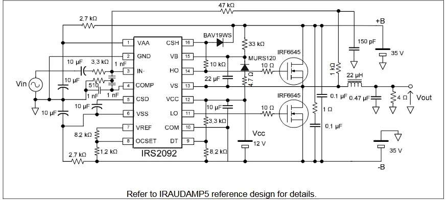
Typical Application Diagram of the IRS2092
The IRAUDAMP5 schematic is a tuned feedback loop. Here is a breakdown of the critical stages shown in the design:- The Floating Input Interface (VAA/VSS): On the input side, the IRS2092 uses a floating input supply (+5V and -5V relative to GND). In a high-power Class D amp, the power ground is incredibly noisy due to high-current switching. By floating the input stage, the IRAUDAMP5 isolates the sensitive audio signal from this switching noise, drastically improving the Signal-to-Noise Ratio (SNR).
- The PWM Modulator and Feedback Loop: Unlike designs that use a separate triangle-wave oscillator, the diagram shows a feedback trace running from the output (before the inductor) back to the input. This feedback loop turns the amplifier into a self-oscillating system. The switching frequency is not fixed; it is determined by the propagation delay through the controller and the MOSFETs, typically tuned to operate around 400kHz.
- The Half-Bridge Power Stage: The design uses two N-Channel MOSFETs stacked between the positive (+B) and negative (-B) high-voltage rails. The IRS2092 drives the high-side FET via the HO pin and the low-side FET via the LO pin. You will also notice a bootstrap diode and capacitor connecting to the VB and VS pins, required to generate the floating voltage needed to drive the high-side gate.
- The Output LC Filter: To the right of the MOSFETs lies the reconstruction filter. This Low-Pass Filter (LPF) removes the 400kHz switching carrier frequency, leaving only the amplified audio signal to drive the speaker. The IRAUDAMP5 design carefully calculates these values to ensure a flat frequency response (20Hz–20kHz) without excessive peaking.
- Integrated Protection Sensing: The design uses the RDS(on) of the MOSFETs themselves as current sense resistors. The CSH pin monitors the voltage drop across the high-side FET, while the OCSET pin sets the threshold for the low-side FET. This “lossless” sensing eliminates the need for large, power-wasting shunt resistors.
Critical Subsystems of the IRS2092
In this section, we will explore the four subsystems of the IRS2092 architecture.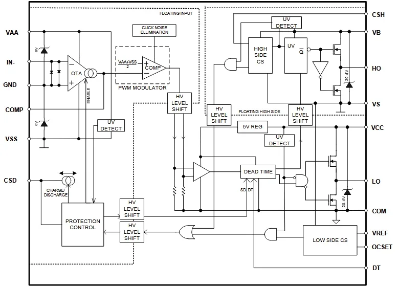
Functional Block Diagram of IRS2092
1. The Output Stage (MOSFETs and Deadtime)
The IRS2092 is a gate driver IC that drives external N-channel MOSFETs for efficient switching. The reference design relies on matching the specific MOSFET characteristics (Gate Charge, RDS(on) ) with the driver’s deadtime settings. The chip allows you to program deadtime via the DT pin. This is the brief pause between switching the high-side and low-side transistors to prevent a short circuit. Too much deadtime increases total harmonic distortion (THD), while too little deadtime risks catastrophic shoot-through.Reference Design Deadtime Settings:
| DT Pin Voltage | Deadtime Mode | Typical Deadtime (ns) | Recommended For |
| > 4.6V (VCC) | DT1 | ~25 ns | GaN FETs or very fast MOSFETs |
| 0.36 x (VCC) | DT2 | ~45 ns | Low Qg MOSFETs (e.g., IRF6645) |
| 0.23 x (VCC) | DT3 | ~75 ns | Medium Power MOSFETs (Standard Use) |
| < 1.0V (COM) | DT4 | ~105 ns | Large High-Power MOSFETs |
2. The Output Filter (LC Reconstruction)
The output filter reconstructs the analog audio waveform from the high-voltage PWM pulses. This is arguably the most critical passive section for audio quality.- Inductor: The reference design typically calls for an inductor with very linear characteristics to minimize distortion. Sagging inductance at high current will cause THD to spike.
- Capacitor: A metalized polypropylene film capacitor is standard for the output filter due to its low dielectric loss and stability.
3. Protection Circuits
One of the IRS2092’s strengths is its integrated bidirectional over-current protection (OCP).- High-Side Sensing: Uses the RDS(on) of the high-side MOSFET sensed via the CSH pin.
- Low-Side Sensing: Uses the RDS(on) of the low-side MOSFET sensed via the OCSET pin.
Design Tip: The reference design sets the trip point using external resistors. If you change your MOSFETs to a type with a different RDS(on), you must recalculate these resistor values to ensure protection triggers correctly.
4. Power Supplies
The IRS2092 requires multiple rails.- B (High Voltage): Powers the MOSFETs (e.g., ±50V).
- VCC (12V-15V) powers the low-side driver and logic. The reference design often uses Zener diodes to derive internal analog front-end power (±5V) from the main VCC to keep the BOM simple.
Layout Guidelines: Managing the Noise
The IRS2092’s high dv/dt switching and large currents make control of parasitic inductance and capacitance critical.1. Grounding: Star Point Topology
The IRS2092 uses two ground references.- GND (Pin 2): Quiet analog ground for the input and error amplifier
- COM (Pin 10): Noisy power ground for the low-side gate driver
Strategy: Keep analog ground and power ground separate and connect them at a single star point, typically at the bulk capacitor or supply return. This prevents switching currents on COM from modulating the analog GND reference.
2. Minimizing the High-Current Switching Loop
The loop formed by the positive bus, the high-side MOSFET, the low-side MOSFET, and the negative bus carries large transient currents.
Strategy: Place high-frequency ceramic decoupling capacitors as close as possible to the high-side MOSFET drain and the low-side MOSFET source to minimize loop area. A small loop reduces EMI and switching-node ringing that can overstress the MOSFETs.
3. Protecting the Feedback Trace
The feedback path to the IN- pin directly affects audio fidelity and is highly noise sensitive.
Strategy: Route the feedback trace away from the switching node (VS) and the output inductor. Prefer routing on a bottom or inner layer with a ground plane above it for shielding, and avoid parallel runs with high-voltage switching traces.
If you’re looking for verified CAD models for the IRS2092 reference guide and the associated power components found in its reference designs, Ultra Librarian helps by compiling all your sourcing and CAD information in one place. Our platform provides verified, ready-to-use footprints, symbols, and 3D models that support all popular ECAD applications, along with sourcing information from worldwide distributors.
Working with Ultra Librarian sets your team up for success, ensuring streamlined, error-free design, production, and sourcing. Register today for free. 


")