
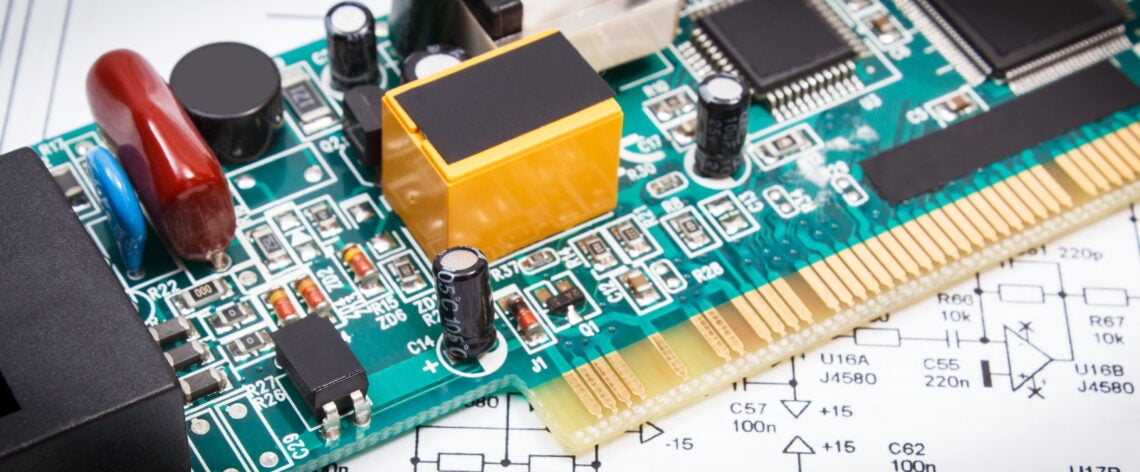
The number of connected IoT devices is expected to grow 14% year over year to 22 billion by the end of 2026, with some analysts projecting it will reach around 39 billion by 2030. Every one of those devices needs a board that packs wireless radios, sensors, and a microcontroller into a form factor that is often smaller than a matchbook. You cannot simply shrink a standard layout and expect it to work. Instead, effective PCB design for IoT devices demands a ground-up strategy tailored to RF performance, ultra-low-power operation, and dense integration. As footprints shrink, electromagnetic interference (EMI) increases, thermal dissipation paths become more restricted, and maintaining stable power delivery becomes more difficult.
The majority of IoT devices run entirely on battery power, which makes power consumption the governing metric of the entire design. Balancing that against other constraints, such as BOM costs, battery capacity limitations, enclosure size restrictions, regulatory compliance (FCC/CE), and long-term environmental reliability, requires deliberate architectural decisions from the first schematic line.
Four Design Constraints Considerations on Every IoT Board
- Miniaturization: Routing complex signals into physical envelopes smaller than a coin.
- Power Efficiency: Achieving sub-microampere deep-sleep currents to extend battery life for years.
- Connectivity: Ensuring reliable radio frequency (RF) transmission despite close component proximity.
- Reliability: Surviving harsh environmental conditions without structural or electrical failure.
Balancing Power, Size, and Cost
Minimizing quiescent current is a major first step in PCB design for IoT devices. When the device enters sleep, the hardware should draw no more than 1-5 µA. Achieving this requires selecting low-dropout regulators (LDOs) rated for operation above 90% efficiency at ultra-low loads, and verifying that every passive component on the rail meets its specified leakage rating.
Physical miniaturization forces a move away from through-hole and standard surface-mount routing. High-Density Interconnect (HDI) technology is mandatory for most modern wearables and compact sensors. System-in-Package (SiP) devices combine the microcontroller, memory, and radio into a single component, drastically reducing the required board area. Routing these fine-pitch components requires microvias, blind vias, and buried vias.
Comparison of Stackup Material Selection For IoT Devices
| Laminate Type | Best For | Trade-off |
| Standard FR-4 | Sub-1 GHz radios, short-range BLE | Low cost; dielectric loss increases sharply above ~1 GHz |
| High-Frequency Laminates (Rogers, PTFE) | 5G cellular IoT, radar up to 28 GHz | Significantly higher material and fabrication costs |
| Hybrid Stack-ups | Mixed-radio designs requiring both RF and digital routing | Balances performance and budget; adds fabrication complexity |
Wireless Connectivity and Antenna Placement
Antenna implementation is where IoT PCB designs most commonly fail in the field, and the physics here are unforgiving. A quarter-wave antenna for 2.4 GHz, the frequency used by Wi-Fi and Bluetooth Low Energy (BLE), calculates to approximately 31.25 mm (roughly 3.1 cm) in free space. You must achieve a precise 50-ohm impedance match between the radio transceiver, the transmission line, and the antenna feed point. Any impedance discontinuity reflects energy back toward the source, reducing range and increasing radiated noise.
Placement discipline is equally important for PCB design for IOT:
- Position the antenna at the edge or corner of the board, away from the main component cluster.
- Clear all copper, ground planes, and traces from every layer within the antenna keep-out zone.
- Never route high-speed digital lines near the RF feed path.
- Verify that the final enclosure design keeps metal fasteners and shielding away from the radiating element.
EMC/EMI Control and Sensor Integration
Mixed-signal IoT boards operate in inherently noisy environments, and layout is your primary mitigation tool. A minimum 4-layer to 6-layer stack-up is recommended for any device incorporating Wi-Fi or BLE. Dedicated, continuous ground and power planes serve as both return paths and inherent shielding against EMI. Jumping straight to 8 layers for a simple BLE beacon, on the other hand, adds manufacturing cost with no measurable benefit.
Make sure to:
- Physically separate analog sensor traces from high-speed digital routing and RF paths.
- Group analog components into their own isolated board sector.
- Route digital signals on inner layers sandwiched between solid ground planes to contain radiated emissions.
A high-speed trace routed over a split in the ground plane forces return current to take a wide, unpredictable path — effectively creating a loop antenna that radiates noise across the entire device.
IoT PCB Design Parameters Reference
| Subsystem | Critical Parameter | Typical Target | Consequence of Ignoring |
| RF Trace | Characteristic Impedance | 50 ohms | Signal reflection, reduced wireless range |
| Power Management | Deep Sleep Quiescent Current | 1 to 5 µA | Premature battery depletion |
| Antenna (2.4 GHz) | Quarter-Wave Length | ~31.25 mm | De-tuned resonance, connection drops |
| High-Speed Digital | Ground Return Path | Continuous, unbroken | High EMI radiation, signal degradation |
| Thermal Management | Copper Pour + Thermal Vias | Per component datasheet | Sensor drift, component degradation during TX bursts |
Hardware Security at the Layout Level
Access to the JTAG/Serial Wire Debug (SWD) debug interface opens up the possibility for an attacker to extract firmware from the device, patch the firmware, and re-flash modified or malicious firmware back into the device. Security should be addressed at the layout phase, not after the fact.
Integrate hardware cryptographic authentication chips early in your schematic to establish a hardware root of trust for secure boot. For debug port hardening, the right approach depends on your microcontroller vendor:
- Leaving JTAG access open after deployment is a security risk; attackers can exploit it to bypass security checks or extract firmware. Consider disabling JTAG access using eFuses once development is complete.
- Some devices lock SWD/JTAG in production for security. Plan a signed unlock flow for service, or provide a secure bootloader so you do not need physical debug on field units.
- For boards where omitting the physical header pads entirely is feasible, this remains the most reliable option. No pads means no probe point.
The specific mechanism (eFuse blow, read-back protection register, or pad omission) varies by silicon vendor. Consult your MCU’s security reference manual before committing to a production strategy.
Common Layout Mistakes to Avoid
Thermal management is the most frequently overlooked issue on low-power IoT boards. Average power may be low, but sudden cellular transmission bursts generate concentrated, localized heat that degrades nearby sensors if copper pours and thermal vias are not implemented. Plan for peak current, not average current.
Beyond thermal issues, watch for these manufacturing pitfalls:
- Placing RF modules immediately adjacent to switching power regulators, which injects broadband noise directly into the transceiver front end.
- Failing to calculate voltage drop across long, thin power traces, which causes microcontroller brownouts during peak current draws, such as Wi-Fi association or cellular registration.
- Routing any trace over a ground plane split, regardless of signal speed — even slow signals create EMI problems when the return path is forced to detour.
- Overcomplicating the PCB design development stack-up unnecessarily, thereby increasing fabrication costs without improving electrical performance.
Design for Manufacturability (DFM)
A working prototype means nothing if it cannot be mass-produced reliably. IoT devices are frequently deployed in harsh environments and subjected to temperature fluctuations, humidity, and vibration. Validate your layout choices against your contract manufacturer’s specific process capabilities before generating final Gerber files.
Wearable devices often require rigid-flex printed circuit boards (PCBs) or irregular board outlines. Develop a sensible panelization strategy early by adding breakaway tabs and fiducial markers that allow automated assembly machines to handle irregular boards without damaging overhanging components. Your manufacturer should approve the panelization plan before you release it to production.
PCB Design for IoT Devices Checklist
Review these items before generating final manufacturing files:
- Is the RF transmission line matched to 50 ohms using controlled impedance routing?
- Are all power delivery paths kept as short and wide as the layout allows?
- Have you verified total deep-sleep leakage current across all passive and active components?
- Are analog sensor zones physically isolated from high-speed digital and RF noise sources?
- Is the JTAG/SWD debug port disabled via eFuse, read-back protection, or by omitting the physical pad for production units?
- Have copper pours and thermal vias been added beneath high-peak-current components?
- Has the panelization strategy been reviewed and approved by your contract manufacturer?
Navigating the engineering constraints of PCB design for IoT devices requires more than just careful routing; it requires precise, verified component data from the start. Whether you’re balancing thermal loads or tuning an RF feed line, having the right CAD models guarantees your layout matches reality. Ultra Librarian provides millions of pre-verified models compatible with popular ECAD applications and connects you directly with worldwide distributors to source parts effortlessly.
Working with Ultra Librarian sets your team up for success, ensuring streamlined and error-free design, production, and sourcing. Register today for free.
Frequently Asked Questions
How many layers should an IoT PCB have?
Most Wi-Fi and BLE devices need 4 to 6 layers to support continuous ground planes and controlled-impedance routing. Simple, low-speed sensor nodes can work on 2 layers. Complex multi-radio cellular gateways often require 8 or more layers, though you should have a concrete electrical reason before adding layers — each one adds cost.
What is HDI in IoT PCB design?
High-Density Interconnect (HDI) refers to manufacturing techniques that enable significantly tighter routing by using microvias, blind vias, and fine-pitch component placement. HDI is essential for shrinking the physical footprint of wearables and compact sensors to the point where standard via-in-pad routing is no longer feasible.
How do I reduce power consumption in the board layout?
Keep power delivery traces short and use a heavier copper weight to minimize resistive drop. Use solid, unbroken ground planes to prevent digital switching noise from waking the microcontroller out of sleep. Select every component, including passives, based on its minimum quiescent current rating, and sum those values at the system level before committing to a battery size. Ensure you choose the right PCB antenna footprints to maximize wireless efficiency without draining excess power.
.


")