
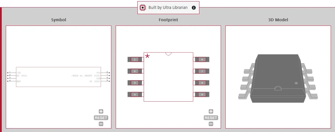
The W25Q128 is a 128-Mbit Serial Peripheral Interface (SPI) Flash memory device providing non-volatile storage for embedded systems, Internet of Things (IoT) devices, and microcontroller-based projects. High-speed memory doesn’t leave much room for guesswork on the PCB side. Implementing a validated W25Q128 SPI NOR Reference Design accelerates development while preventing data corruption caused by poor signal integrity or unstable power delivery.
Such a reference design provides engineers with a proven baseline for space-constrained and power-limited applications. Once the design is validated, the part itself is easy to source through distributor partners like Digi-Key, keeping the path from schematic to finished board short.
Pin Configuration and SPI Modes
The W25Q128 supports multiple SPI configurations, scaling data throughput to meet system requirements.
- Standard SPI: Uses four primary signals: Clock (CLK), Chip Select (/CS), Data In (DI), and Data Out (DO).
- Dual SPI: Converts the DI and DO pins into bidirectional I/O pins (IO0, IO1), doubling the transfer rate without requiring extra microcontroller pins.
- Quad SPI (QSPI): Utilizes the Write Protect (/WP) and Hold (/HOLD) pins as additional I/O lines (IO2, IO3), quadrupling data throughput compared to standard SPI.
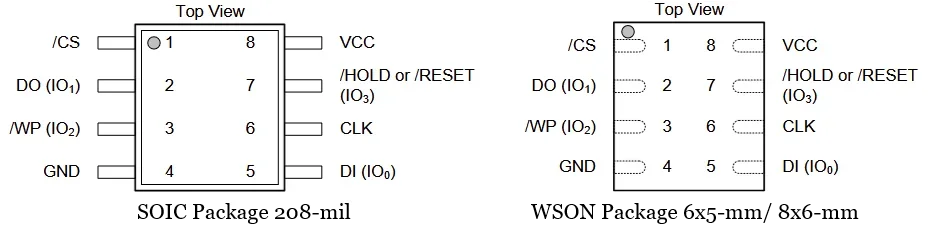
W25Q128 Pinout
| Pin Number | Standard SPI Function | Quad SPI Function | Purpose |
| 1 | /CS | /CS | Active-low Chip Select |
| 2 | DO | IO1 | Data Output / Bidirectional I/O 1 |
| 3 | /WP | IO2 | Write Protect / Bidirectional I/O 2 |
| 4 | GND | GND | System Ground |
| 5 | DI | IO0 | Data Input / Bidirectional I/O 0 |
| 6 | CLK | CLK | Serial Clock |
| 7 | /HOLD | IO3 | Pause Communication / Bidirectional I/O 3 |
| 8 | VCC | VCC | Power Supply |
Signal Integrity and Routing for High-Speed SPI
Quad SPI mode pushes clock frequencies up to 133 MHz, fast enough that sloppy routing will bite back with reflections and timing mismatches.
- Length Tuning: Match trace lengths for the CLK and IO0-IO3 data lines. Such length tuning ensures signals arrive simultaneously, preventing setup and hold time violations.
- Impedance Management: For long traces or high clock frequencies, route SPI lines with consistent trace widths to avoid sudden impedance discontinuities.
- Reference Planes: Route high-speed traces over an unbroken solid ground plane. Avoid routing over split planes, as gaps create impedance discontinuities and increase electromagnetic interference (EMI).
- Trace Minimization: Keep trace lengths as short as possible to minimize parasitic capacitance and signal degradation.
Power Supply Decoupling of W25Q128 SPI NOR Reference Design
Every high-speed read or write cycle throws a quick current spike at the power rail, so solid decoupling at the VCC pin isn’t optional; it’s what keeps the voltage steady.
- Place a 0.1 µF low-ESR (Equivalent Series Resistance) ceramic capacitor directly adjacent to the VCC and GND pins.
- Keeping the decoupling trace loops minimal reduces parasitic inductance.
- For designs anticipating heavy erase or program cycles, add a secondary 1.0 µF or 4.7 µF bulk capacitor near the flash memory device to support peak current demands without causing voltage droop.
Package Selection: SOIC vs. WSON Package
Relying on a verified W25Q128 SPI NOR Reference Design eliminates guesswork during schematic capture and layout. Instead of calculating trace impedances or experimenting with capacitor placement, designers can implement a known-good configuration. Engineers should select physical packages based on manufacturing capabilities and available board space. The W25Q128 is commonly available in two primary formats:
- SOIC (Small Outline Integrated Circuit): Features exposed gull-wing leads. Such a physical package simplifies hand-soldering and manual inspection, making it an excellent choice for low-volume prototyping and debugging.
- WSON (Very Thin Small Outline No-Lead): Offers a significantly smaller physical footprint with bottom-facing contact pads. The exposed center thermal pad improves heat dissipation for thermally constrained environments. However, manufacturing requires exact solder paste stencils and automated reflow ovens.
Distributors such as Digi-Key and Octopart typically stock both SOIC and WSON variants, making it easy to check real-time availability before committing to a package choice. If you’re looking for CAD models for common components or W25Q128 SPI NOR Reference Design, Ultra Librarian helps by compiling all your sourcing and CAD information in one place.
Register today to start building reliable embedded systems.
Working with Ultra Librarian sets your team up for success by ensuring streamlined, error-free design, production, and sourcing. Register today for free.

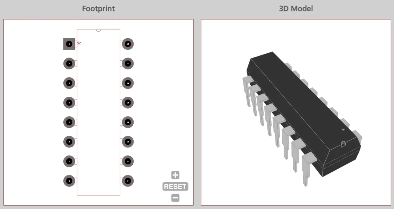
 If you’re looking for any of our component footprints or models, we have readily available and free options for you and your design team. Search our library for the solution you’ve been looking for.