Engineering departments face immense pressure to release hardware quickly, which only grows as teams scale across multiple global sites. When electrical engineers work independently without a unified approach, individual design preferences creep into the process. These inconsistencies often surface only after fabrication, when mismatched conventions between engineers lead to manufacturing delays.
Corporate PCB design standards solve this problem by giving every engineer, regardless of location, the same set of rules to design against. A standardized approach ensures consistency across product lines and reduces common layout errors. In turn, this accelerates time-to-market by removing guesswork during the layout phase. These rules may feel limiting at first, but they pay off during fabrication. When a manufacturing plant knows exactly what to expect from a board layout, yields increase, and the cost per board decreases.
Centralizing Component Libraries for Consistency
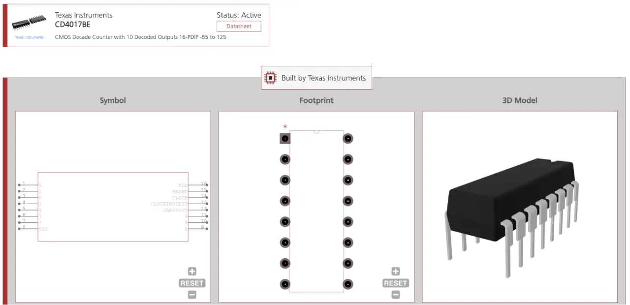
A reliable foundation for hardware development relies on single-source component data, yet it breaks down as soon as individual engineers begin creating their own local libraries. For example, a slightly oversized surface-mount pad might cause a small passive component to tombstone during reflow soldering. These risks are why enterprises must mandate centralized component libraries to ensure uniform footprints and schematic symbols across all design teams.
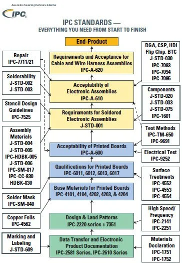
To maintain consistency across thousands of components, enterprises typically base their library rules on industry standards. The organization known as IPC (originally the Institute of Printed Circuits) is now the Global Electronics Association, and it provides exact specifications for library creation. For instance, the IPC-7351 standard specifies the generation of surface-mount footprints. Following IPC-7351 ensures proper solder fillets during the reflow process.
Enterprise libraries should enforce such rules universally. Designers should not guess pad sizes based on a manufacturer’s suggested layout if it conflicts with IPC guidelines. Accordingly, creating standard symbols is equally important. When schematic symbols follow consistent pin naming conventions and visual structures, design reviews become much faster. Engineers can read the schematic like a standardized blueprint rather than interpreting a unique drawing style.
Centralized libraries offer specific advantages for large teams:
- Consistent pin mapping between schematic symbols and layout footprints.
- Accurate 3D STEP models for mechanical interference checking.
- Verified manufacturer part numbers (MPNs) tied directly to company-specific internal part numbers.
- Standardized courtyard outlines to prevent placement collisions on densely packed boards.

Defining Corporate PCB Design Standards for Universal Rules
After securing the library, engineering teams must define universal design rules. The exact corporate PCB design standards will vary based on product requirements. For example, a consumer wearable requires a vastly different layer stack-up than a high-power industrial motor controller. However, every organization should establish baseline requirements for:
- Standard trace width classes for different current levels.
- Minimum trace-to-trace, trace-to-pad, and copper-to-edge clearances.
- Approved layer stack-ups for common board configurations.
- Default via sizes, annular rings, and drill tolerances.
For trace widths, engineers should calculate current-carrying capacity using the IPC-2152 standard. Notably, many older calculators rely on the outdated IPC-2221 nomographs, which often provide misleadingly optimistic estimates for internal layers. The newer IPC-2152 standard accounts for copper thickness, ambient temperature, and board material. Understanding thermal management can help prevent traces from delaminating under heavy loads.
Stack-up design heavily influences signal integrity and electromagnetic compatibility (EMC), making it an important part of any corporate PCB design standard. Rather than creating a new layer arrangement for every project, many organizations maintain approved and validated stack-up templates for manufacturing and EMC performance. Reusing these proven configurations improves design consistency and reduces risk across product lines. The following eight-layer controlled-impedance stack-up illustrates a standardized configuration commonly used in complex enterprise hardware.
Example 8-Layer PCB Stack-Up Configuration
| Layer | Type | Copper Weight | Material | Thickness |
| 1 | Top Signal | 1 oz | FR408HR | 1.4 mil |
| 2 | Ground Plane | 1 oz | Prepreg | 1.4 mil |
| 3 | Inner Signal | 0.5 oz | Core | 0.7 mil |
| 4 | Power Plane | 1 oz | Prepreg | 1.4 mil |
| 5 | Ground Plane | 1 oz | Core | 1.4 mil |
| 6 | Inner Signal | 0.5 oz | Prepreg | 0.7 mil |
| 7 | Ground Plane | 1 oz | Core | 1.4 mil |
| 8 | Bottom Signal | 1 oz | Prepreg | 1.4 mil |
Universal layout constraints often include the following guidelines:
- Minimum trace width and spacing for digital signals (e.g., 4 mil width / 4 mil space).
- Specific via drill sizes and annular ring requirements to prevent breakout during drilling.
- Differential pair spacing and stack-up to maintain 90-ohm USB or 100-ohm Ethernet impedance targets.
- Copper pour clearance distances to avoid shorts during wave soldering.
- Maximum uncoupled length for high-speed differential pairs.
Enforcing Rules with Automated Design Rule Checking
Creating rules solves only half the problem. Engineers must also enforce the established guidelines. Automated design rule checking (DRC) acts as the final gatekeeper before releasing Gerber files to a manufacturer. A poorly configured DRC setup allows errors to slip through to the fabrication house. By the time a factory engineer flags the error, the project has already lost days of valuable time.
To prevent such delays, modern Electronic Computer-Aided Design (ECAD) software can automatically enforce corporate PCB design standards during routing. By loading a predefined constraint file, the software prevents designers from placing traces too close together. The automated DRC system prevents violations before physical connections are even made. Real-time DRC feedback provides immediate visibility when a design violates predefined constraints. If a designer attempts to route a 5-volt power trace too close to a sensitive analog signal, the ECAD tool refuses to complete the connection.
Additionally, enterprises should configure batch DRCs to check for complex manufacturing issues, such as acid traps or solder mask slivers. These batch checks run after the layout is fully routed.
- Acid trap detection to prevent pooling of etching chemicals during fabrication.
- Solder mask sliver checks to ensure the mask does not flake off between closely spaced pads.
- Silkscreen over pad checks to prevent ink from contaminating solder joints.
- Creepage and clearance verification for high-voltage isolation boundaries.
- Unplated through-hole (NPTH) clearance verifications to prevent hardware mounting screws from shorting internal planes.
Strategies for Cross-Functional Collaboration and Auditing
While automated checks prevent many design errors, enterprise hardware development also depends on communication between engineering disciplines. Since the mechanical team needs accurate board outlines and component heights, electrical engineers must collaborate closely with mechanical engineers.
Using the Incremental Design Exchange (IDX) format facilitates bidirectional communication between ECAD and Mechanical Computer-Aided Design (MCAD) software. When the engineer moves a mounting hole in the mechanical 3D modeling tool, the ECAD software prompts the electrical engineer to accept the change. Bidirectional ECAD-MCAD communication reduces the need for manual DXF file exports.
Regular standard audits help maintain engineering excellence because technology changes rapidly. A working design rule for rigid FR4 boards might fail for rigid-flex designs. A footprint created for leaded solder might bridge when used with a modern lead-free paste. Consequently, the engineering management team should review the established corporate standards annually.
During an audit, teams should review specific areas:
- Component obsolescence rates within the central library.
- Feedback from assembly houses regarding frequent Engineering Queries (EQs).
- Updates to IPC standards affecting footprint generation.
- New material availability for high-speed digital designs.
- Yield reports from the factory floor identifying common failure points.
If the assembly house repeatedly flags the same footprint for having too much solder paste, the engineering team must update the library. Closing the feedback loop between manufacturing and design guarantees continuous improvement.
Establishing and maintaining corporate PCB design standards requires a reliable foundation of verified component data. Ultra Librarian provides instant access to millions of prebuilt footprints, schematic symbols, and 3D models, and integrates seamlessly with popular ECAD applications. Engineers can quickly source accurate parts from worldwide distributors without wasting hours drawing custom pads. Start building a unified, error-free component library for the enterprise engineering team today.
Working with Ultra Librarian sets your team up for success by ensuring streamlined, error-free design, production, and sourcing, which is the same precision that strong corporate PCB design standards demand. Register today for free.



 If you’re looking for any of our component footprints or models, we have readily available and free options for you and your design team. Search our library for the solution you’ve been looking for.