PCB USB C Connector: Important Design Guidelines

View of PCB USB-C male plug.

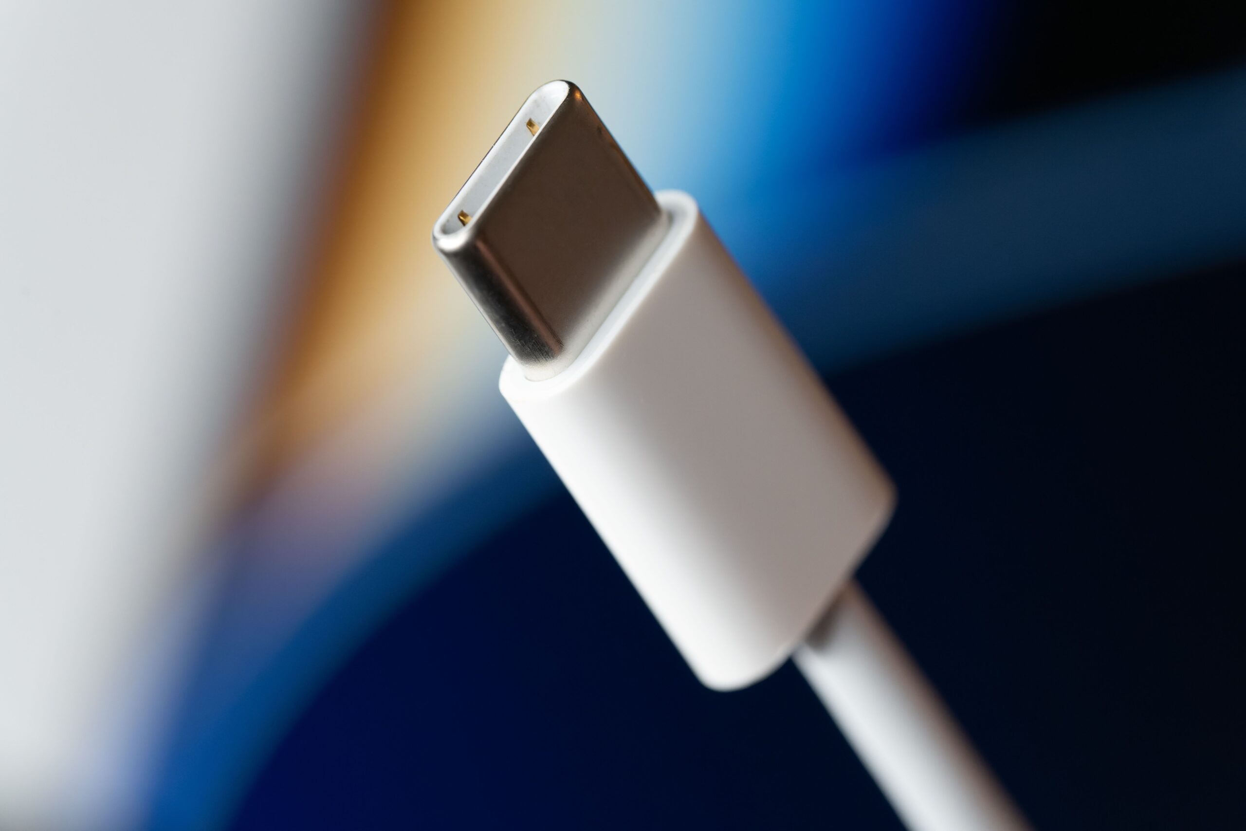
PCB USB-C Connectors are ubiquitous for their fast charging and reconfigurable high-speed data transfer.

As the latest update to the USB connector type format, USB-C offers unparalleled ubiquity across electronics for data transfer and power charging. From the designer’s perspective, USB-C has some additional considerations to weigh during layout to prevent poor performance. For any PCB USB-C connector implementation, the following design best practices will ensure excellent manufacturability and end-user satisfaction.

PCB USB-C Connector Layout Strategies

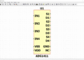
The pinout for USB-C, shown below, is standardized; however, the mechanical outline is not.

PCB USB-C Connector Pinout
Pin Name Function Pin Name Function
A1 GND Return/voltage reference B1 GND Return/voltage reference
A2 TX1+ USB3.1 transfer B2 TX2+ USB3.1 transfer
A3 TX1- USB3.1 transfer B3 TX2- USB3.1 transfer
A4 VBUS Power B4 VBUS Power
A5 CC1 Detection B5 CC2 Detection
A6 D+ USB2.0 transfer B6 D+ USB2.0 transfer
A7 D- USB2.0 transfer B7 D- USB2.0 transfer
A8 SBU1 Alternate mode B8 SBU2 Alternate mode
A9 VBUS Power B9 VBUS Power
A10 RX2- USB3.1 transfer B10 RX1- USB3.1 transfer
A11 RX2+ USB3.1 transfer B11 RX1+ USB3.1 transfer
A12 GND Return/voltage reference B12 GND Return/voltage reference

While general strategies are applicable for all versions of the USB-C connector footprints, the mid-mount SMT connector with EMI ground shielding is arguably the most difficult to route. 

  • Footprint verification – Designers need to ensure the accuracy of the footprint before soldering to minimize rework and yield losses. For long-term solder joint health, check the component’s planarity against the footprint (this will minimize stress/strain at the contact points).
  • Via fanout – In most 2- and 4-layer designs with high-density interconnect (HDI) philosophies, vias are necessary for signal breakout because the combination of tightly-spaced pads and nearby through-hole pins reduces potential routes. 8/16-mil vias (8-mil hole, 16-mil pad) and 3-mil net spacing should provide adequate room for fanout between and around the pin rows. Avoid via-in-pad for USB-C fanout: in addition to being a cost adder, the narrow width of the pads versus the via diameter can cause uneven solder distribution during assembly.
  • Differential pairs – Start by routing the SSRX/TX differential pairs on the top and bottom of the board layout. Regarding signal integrity, these are the most critical nets, and routing these first (or at least routing the breakout from the footprint) will reduce impedance by shortening differential pair traces and length-tuning
  • Power pour – USB-C connectors have a considerably high current draw of five amps. Designers will want to place ample copper to keep the impedance low for low electrical/thermal impedance. The copper can be all internal using an oversized pour on a split-plane layer combined with a stitching pour on the top/bottom layer or exclusively on the top/bottom. Copper pours on the outer layers don’t require as much space for the same electrical/thermal performance, but designers need to be more considerate with outer-layer fanout. Copper pours spanning the inner and outer layers require a via array to minimize impedance.
  • Misc. – Lastly, designers will want to use a ground pour on the outer layers to ensure signal integrity and provide a good grounding for the chassis. For maximum protection, place ESD components as close as possible to the connector on both sides of the board.

Expansive Library Support with Ultra Librarian

PCB USB-C connector layouts can be challenging due to the numerous differential pairs and tight spacing between pin rows; however, a clever designer can accurately navigate the layout given some initial design tips.  The best first step for any designer is to verify the footprint data of the USB-C connector and any supporting components. With millions of verified footprints and additional ECAD data, Ultra Librarian accelerates designs while ensuring manufacturability. Interested in learning more? Sign up for free with Ultra Librarian and see how your design workflow can flourish.

Working with Ultra Librarian sets up your team for success to ensure streamlined and error-free design, production, and sourcing. Register today for free.

UL-Icon.png

The Ultra Librarian Team

Ultra Librarian offers the world’s largest PCB CAD library, putting cutting-edge materials at your fingertips so you can build better products faster—all for free.

Join Our Newsletter

Subscribe to our newsletter to receive the latest news, and important updates

Name(Required)

Related Posts

If you’re looking for any of our component footprints or models, we have readily available and free options for you and your design team. Search our library for the solution you’ve been looking for.

IC Manufacturers

Working with us allows you to target the right audience for your component, provide content to nurture them along their design process, and analyze how your parts are being received and used.

Electronic Component Industry Trends 2024

Download Now to read more about the most impactful drivers of IC component innovation.

Part Details

Pricing by

Free Design Resources

Ultra Librarian is the worlds largest online – and always free – PCB CAD library. Build products better, faster, and more accurately with easy access to vendor-verified symbols, footprints, and 3D models. Register today to start searching the right components for your next design.

Recommended