PCB Design Impacts Jitter
Jitter, a timing deviation, is a concern in high-speed digital electronics and mixed-signal systems. Excessive jitter reduces timing margins, leading to setup/hold violations, bit errors, and overall signal integrity issues in printed circuit board (PCB) designs. Understanding and mitigating jitter in PCB design is crucial for ensuring that electronic products function as intended. This article discusses jitter, including its sources and effects, and outlines strategies for mitigation.
Techniques for Characterizing Jitter in PCB Design
| Tool/Technique | Primary Function | Key Metrics Obtained |
| Oscilloscopes | Visualize waveforms, generate eye diagrams, and perform histogram analysis | RMS Jitter, Peak-to-Peak Jitter, Eye Width/Height * |
| Spectrum Analyzers | Measure phase noise in the frequency domain | Phase Noise Spectral Density |
| Dedicated Jitter Analyzers | Decompose total jitter into its random and deterministic components | RMS Jitter, Peak-to-Peak Jitter, Random Jitter (RJ), Deterministic Jitter (DJ), Total Jitter (TJ) |
*RMS Jitter: standard deviation of timing variations
*Peak-to-Peak Jitter: maximum observed timing variation
*Eye width/height: setup/hold margins. See sections below for more about each.
Jitter: Definition and Classification of Timing Imperfections
Jitter is the dynamic deviation of event instants in a signal from their ideal position in time, excluding modulation components below 10 Hz. This measurable error directly impacts circuit operation and communication.
Types of Jitter in PCB Design
Jitter is generally classified as follows:
- Absolute Jitter: The deviation of a clock edge from a perfect, ideal reference clock.
- N-period Jitter: The variation in cycle duration over a specified number (N) of consecutive periods. For N=1, this is called period jitter.
- Random Jitter (RJ): Unbounded timing variations typically originating from thermal noise or semiconductor flicker noise. RJ follows a Gaussian distribution.
- Deterministic Jitter (DJ): Bounded timing variations with identifiable causes. Examples include inter-symbol interference (ISI), duty cycle distortion (DCD), and crosstalk. DJ exhibits non-Gaussian probability distributions.
- Total Jitter (TJ): The combined effect of all jitter components, often statistically derived from RJ and DJ.
RMS Jitter
Root-mean-square (RMS) jitter represents the statistical standard deviation of timing variations relative to the ideal edge. It quantifies the random component of jitter and is widely used for comparing oscillator and clock distribution quality.
Peak-to-Peak Jitter
Peak-to-peak jitter measures the maximum observed timing deviation over a given sample. Because it depends heavily on sample length and captures rare events, it is useful for evaluating worst-case timing margins in digital systems.
Eye Width/Height
Eye height indicates vertical noise margin, while eye width indicates horizontal (timing) margin. Eye width is directly tied to setup and hold time, making it a key indicator of a system’s tolerance to jitter and noise.
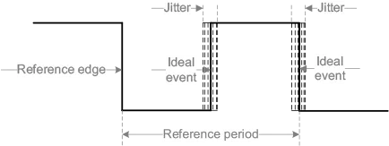
Time Domain Representation of Jitter
Sources of Jitter in PCB Design
Jitter in PCB design arises from various design and environmental factors within a PCB:
| Source of Jitter | Description |
| Power Supply Noise | Ripples, transients, or ground bounce on DC power rails can couple into clock generation/distribution circuits. Voltage fluctuations alter switching thresholds, causing timing shifts in output edges. |
| Crosstalk | Electromagnetic coupling (capacitive or inductive) between adjacent traces. Aggressor signals induce noise on victim traces, adding timing variations, which is common in dense layouts with parallel routing. |
| Impedance Mismatches & Reflections | Discontinuities in transmission paths (trace width changes, poor via design) cause reflections. These lead to ringing, false edges, or shifted transitions that contribute to jitter. |
| PCB Material Properties | Variations in dielectric constant (Er), loss tangent (tan δ), copper roughness, and thermal effects alter the propagation speed and attenuation, adding jitter. |
| Component Characteristics | Intrinsic jitter of oscillators, phase-locked loops (PLLs), clock buffers, and transceivers. Vendors like Cirrus Logic provide low-jitter devices critical for high-performance timing (e.g., audio). |
| Suboptimal Layout Practices | Inaccurate trace length matching in critical clock paths or differential pairs. Improper via usage causing impedance discontinuities or stubs. Inadequate power and ground plane integrity. Suboptimal component placement affecting return paths. |
Effects of Jitter on System Performance
Uncontrolled jitter can degrade system functionality and performance:
- Reduced Performance: Clock jitter can lead to incorrect data sampling in digital circuits, resulting in setup and hold time violations.
- In Analog-to-Digital Converters (ADCs) and Digital-to-Analog conversion, an increase in jitter leads to degraded signal-to-noise ratio (SNR) and the introduction of distortion.
- Jitter directly limits the maximum achievable data rates for high-speed interfaces (e.g., PCIe, USB, Ethernet) by consuming timing budgets.
- Increased Bit Error Rate (BER): High jitter significantly increases the probability of bit errors in high-speed serial communication links.
- Electromagnetic Interference (EMI) Complications: Jitter spreads the spectral energy of a clock signal across a wider frequency band. This spectral spreading can complicate meeting electromagnetic compatibility (EMC) and EMI compliance regulations.
- Debugging Complexity: Jitter-related issues are often intermittent, temperature-dependent, and challenging to reproduce, leading to prolonged development and troubleshooting cycles.
Strategies for Jitter Mitigation in PCB Design
Mitigating jitter in PCB design requires a comprehensive approach encompassing design principles, careful component selection, and thorough verification:
| Area of Focus | Mitigation Strategies |
| Power Integrity (PI) | Design stable power delivery networks (PDNs) Place decoupling capacitors near IC pins Ensure low impedance power/ground planes across frequency ranges. |
| Signal Integrity (SI) | Implement controlled impedance routing Minimize stubs Use proper termination Route differential pairs with tight coupling and length matching Minimize vias in clock paths |
| Clock Distribution | Utilize dedicated clock layers for isolation Use clock buggers designed to add little additional jitter Incorporate PLLs for clock cleaning and synthesis |
| Component Selection | Select high-quality oscillators, clock generators, and clock management ICs with verified low jitter specifications (e.g., Cirrus Logic’s Audio Clock Generation products). |
| Simulation & Verification | Employ pre-layout and post-layout SI/PI analysis tools to model crosstalk, reflections, and power supply noise, identifying jitter sources early |
Cirrus Logic and Ultra Librarian
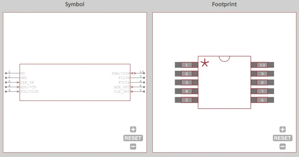
Cirrus Logic’s CS2500 Symbol and Footprint Data from UltraLibrarian
Cirrus Logic is a leader in high-performance mixed-signal circuits, particularly in the audio sector. Cirrus Logic focuses on minimizing jitter in components like ADCs, DACs, and clock generators. Their “Audio Clock Generation and Jitter Reduction” solutions exemplify their commitment to offering precise timing for jitter-sensitive applications.
Ultra Librarian provides a comprehensive library of accurate, high-quality CAD models (symbols, footprints, and 3D models) for millions of components, including those from Cirrus Logic. Access to verified models for low-jitter clocking solutions and high-performance mixed-signal ICs simplifies design integration. This accelerates the design process, reduces manual part creation errors, and facilitates accurate simulations, contributing to the development of low jitter in PCB design.
Working with Ultra Librarian sets your team up for success, ensuring streamlined and error-free design, production, and sourcing. Register today for free.