
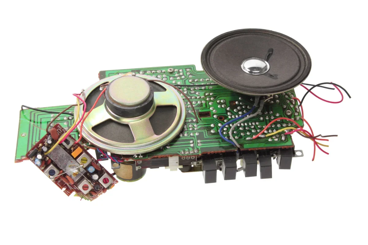
PCB of Radio Cassette Player
For anyone who values a precise audio experience, from recorded music to live sound, the quality of that experience is built upon many technical elements. A major part of this is PCB design. Analog signals, digital data streams, and power-delivery networks coexist on a single board, and they all impact sound quality. Managing the interaction of the various components in a PCB design is essential for high-quality audio without noise, distortion, or signal degradation. Innovations from companies like Cirrus Logic aim to simplify these design complexities, and resources such as Ultra Librarian provide engineers with the tools needed for accurate implementation.
Noise Sources in Audio PCBs and Mitigation Strategies
| Performance Factor | Description | Mitigation Strategy |
| EMI/RFI | External or internal electromagnetic/radio frequency interference, often from switching power supplies, high-speed digital circuits, or external fields. | Shielding (ground planes, shield cans), optimal trace routing. |
| Crosstalk | Signal coupling between adjacent traces. | Trace spacing, orthogonal routing, ground planes. |
| Power Supply Ripple | Unwanted AC components on DC power rails. | Multi-capacitor decoupling networks, stable linear/LDO regulators. |
| Voltage Drops (IR Drop) | Decrease in DC voltage along power traces due often to trace resistance and high current draw. | Wider power traces, multiple power vias, localized bulk capacitance. |
| Ground Bounce | Voltage fluctuations in the ground reference due to rapidly switching currents, especially in digital circuits. | Solid, low-impedance ground planes; dedicated ground vias for ICs; decoupling. |
| Switching Noise | Generated by active components (e.g., regulators, digital ICs) during their switching transitions. | Filtering (RC/LC networks), physical isolation, localized decoupling. |
| Reflections | Signal bounces back due to impedance mismatches in traces, distorting the waveform. | Controlled impedance routing, proper trace termination (e.g., series/parallel resistors). |
| Attenuation | Signal strength loss over distance, resulting in reduced amplitude and a lower signal-to-noise ratio. | Short trace lengths, appropriate conductor width for current/frequency, and low-loss dielectric materials. |
| Thermal Noise | Inherent random noise generated by the thermal agitation of charge carriers in resistive components (Johnson-Nyquist noise). | Bandwidth reduction (filtering), selection of low-noise components (e.g., precision resistors, low-noise op-amps). |
Achieving Clarity: PCB Design in Audio
Engineers employ various techniques to achieve high-quality sound from audio circuits. These methods involve careful planning and precise physical layout.
Grounding Strategies for Quiet Circuits
Grounding schemes are fundamental for achieving noise-free audio PCBs.
- Solid Ground Plane: A continuous ground plane provides a low-impedance return path for currents and shields sensitive circuits from radiated noise.
- Analog and Digital Ground Separation: Isolating analog and digital grounds prevents noisy digital currents from affecting sensitive analog signals. This often involves partitioning the board and connecting grounds at a single, controlled point, if necessary.
- Star Grounding: In circuits with high currents, such as headphone amplifiers, star grounding can be effective. This method designates a single central ground point, to which all other ground connections (for various circuit sections) route directly. This prevents ground currents from different circuit parts from creating voltage differentials across the ground plane.
Optimized Layout and Component Placement
Component placement and board partitioning are important for minimizing interference.
- PCB Partitioning: Physically separating analog and digital areas reduces interference.
- Short, Direct Signal Paths: Keeping signal traces short and direct minimizes their ability to act as antennas, reducing both emission and susceptibility to interference, thus preserving signal integrity.
- Component Isolation: Noisy components, such as switching power supplies and high-speed digital ICs, should be placed as far away from sensitive analog circuitry as practically possible.
Power Supply Decoupling
Even with effective grounding, a noisy power supply will affect audio quality.
- Decoupling Capacitors: These capacitors act as local energy reservoirs, providing instantaneous current when an IC demands it and shunting high-frequency noise to ground.
- Placement: Decoupling capacitors must be placed as close as possible to the power pins of the integrated circuits they serve, often within millimeters.
- Capacitor Network: A combination of capacitor values is typically used. Small ceramic capacitors (e.g., 0.1µF) filter high-frequency noise, while larger electrolytic or tantalum capacitors (e.g., 10µF to 100µF) handle lower-frequency ripples and provide bulk capacitance.
- Routing Strategy: A common routing strategy, often referred to as “Via, Cap, Pin,” ensures that the power trace connects to the decoupling capacitor first, then proceeds directly to the IC pin, providing the shortest path for noise bypass.
Signal Routing for Integrity
The design of signal traces also requires specific attention.
- Controlled Impedance Routing: This is important for higher-frequency audio signals and their harmonics. It involves matching trace impedance to the source and load, preventing signal reflections, and ensuring traces behave as uniform transmission lines.
- Trace Geometry: Avoid sharp 90-degree corners in traces, as these create impedance discontinuities and can increase EMI. Use 45-degree angles or smooth curves instead.
- Shielding: Surround sensitive signal traces with ground planes. Sandwiching the signal traces between two ground layers in a multi-layer board can reduce both signal emissions and susceptibility to external noise.
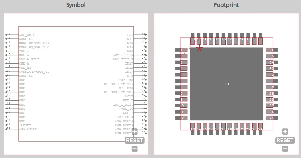
Cirrus Logic’s CS5304P Symbol and Footprint on Ultra Librarian
Beyond Basic Techniques: Advanced Solutions
High-performance audio systems often require a combination of diligent board layout and intelligent component integration.
Cirrus Logic’s Hybrid Gain Control (HGC), featured in their CS530xP family of Pro Audio ADCs, offers an example of such integration. This technology addresses the “pop” and “zipper noise” that can occur during gain adjustments in digitally controlled microphone preamps. HGC integrates analog zero-cross detection and synchronized digital gain control directly into the ADC chip. This enables gain changes to occur smoothly, synchronized with the audio signal’s zero-crossing point, which eliminates artifacts and makes digital control feel similar to traditional potentiometers. This demonstrates how intelligent IC design can complement PCB design in audio practices, simplifying hardware and software while improving the user experience.
The Challenge of Gain Adjustment
Traditionally, adjusting the gain in digitally controlled analog signal paths, particularly in sensitive applications such as microphone preamps, has presented a design challenge. When gain changes occur abruptly or at arbitrary points in the audio waveform, they introduce transient artifacts. The most common of these are:
- Pop Noise: A sudden, audible click or thud resulting from a DC offset shift or rapid change in signal level.
- Zipper Noise: A series of small, rapid “zips” or “crackle” sounds occurring as the digital gain steps through its values, particularly noticeable with fine gain adjustments. This is often due to the instantaneous, step-like changes in voltage from the DAC controlling the analog gain stage.
Engineers traditionally tackled these issues with complex external circuitry, such as digitally controlled potentiometers (DCPs) or VCAs (Voltage Controlled Amplifiers) combined with zero-crossing detection circuits, often requiring many discrete components, careful calibration, and intricate software timing. All of this added to board space, component count, intricate trace routing, cost, and overall design complexity.
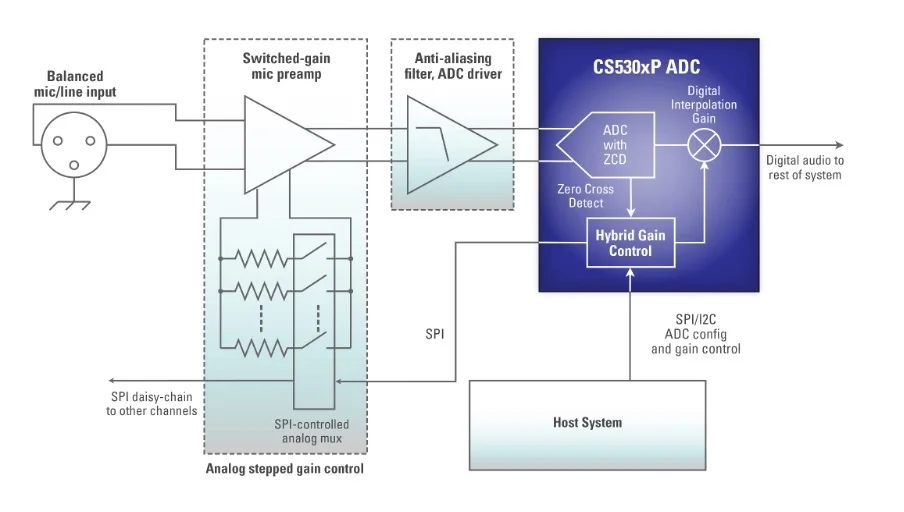
Mic preamp gain control with Cirrus Logic HGC
Hybrid Gain Control: An Integrated Solution
Cirrus Logic’s HGC technology provides an integrated solution to these problems. Instead of relying on external components and complex software management, HGC embeds gain adjustment functionality directly within the ADC.
- Analog Zero-Cross Detection: The core of HGC is an analog zero-cross detection circuit, which continuously monitors the input audio signal. This circuit identifies the moment the audio waveform crosses the 0V reference point.
- Synchronized Digital Gain Control: When a digital gain change command is issued (e.g., via SPI), the ADC’s internal logic doesn’t apply the change immediately. Instead, it waits for the next detected zero-crossing point of the analog input signal. Once the zero-crossing is confirmed, the digital gain value is updated and applied to the analog gain stage within the ADC, ensuring a smooth, non-disruptive transition.
This precise synchronization prevents the instantaneous voltage steps that cause pop and zipper noise, effectively “smoothing” the digital gain control into an analog-like feel.
Benefits of Hybrid Gain Control for PCB Design and System Integration
| Benefit | Impact on Design and System |
| Reduced Component Count | Integrated ADC functionality reduces external discrete components (e.g., control logic, switches), resulting in smaller PCB footprints and lower Bill of Materials (BOM) costs. |
| Simplified Layout | Fewer external components lead to simpler routing, reducing noise, crosstalk, and layout-induced performance issues. |
| Faster Development Cycle | Less time spent debugging transient gain artifacts accelerates design and testing, enabling focus on overall audio performance. |
| Improved Performance and Reliability | Centralized timing and synchronization within the IC ensure consistent performance and enhance system reliability by reducing discrete component failure points. |
| Compatibility and Flexibility | Compatibility with standard mic preamp architectures and common digital interfaces (e.g., daisy-chain SPI) offers broad system design flexibility. |
Implementing these techniques of PCB design in audio, from precise grounding to complex signal routing and power decoupling, requires access to accurate and comprehensive component data. Ultra Librarian offers engineers access to millions of free symbols, footprints, and 3D models in over 30 CAD formats. This makes it straightforward to find and integrate components, including those from partners like Cirrus Logic. By offering verified, ready-to-use models, Ultra Librarian helps streamline the design process, reduces potential errors, and allows engineers to focus on refining their audio circuits.
Working with Ultra Librarian sets your team up for success, ensuring streamlined and error-free design, production, and sourcing. Register today for free.


")
")
")
")