The 555 timer is one of the most recognizable chips in electronics, used for pulse generation, delays, and oscillation. However, with multiple manufacturers producing variants such as the NE555, LM555, and CMOS versions, determining the exact specifications can be tricky. This guide simplifies the 555 timer datasheet, breaking down the universal pinouts, timing calculations, and operating modes to help you design with confidence.
555 Timer Datasheet Pinout and Functions
Regardless of the manufacturer, the standard single 555 timer usually comes in an 8-pin package (DIP-8 or SOIC-8).
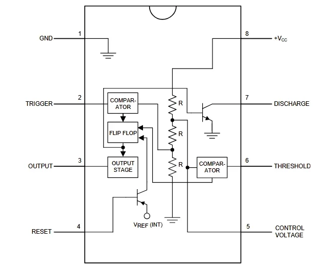
555 Timer Pin Description
| Pin # | Name | Function |
| 1 | GND | Ground reference (0V). |
| 2 | Trigger | When this pin drops below ⅓ Vcc, the output goes HIGH and timing starts. |
| 3 | Output | Capable of sinking or sourcing current (up to 200mA for bipolar versions). |
| 4 | RESET | Active-low reset. Forces output LOW. Connect to Vcc if not used. |
| 5 | Control Voltage | Allows external modification of threshold voltage. Usually decoupled to ground with a 10nF capacitor. |
| 6 | Threshold | When this pin exceeds ⅔ Vcc , the output goes LOW. |
| 7 | Discharge | Connected to the collector of an internal transistor; used to discharge the timing capacitor. |
| 8 | Vcc | Supply Voltage (Typically 4.5V to 15V). |
Operating Modes and Timing Calculations
The datasheet typically details three modes of operation. To use them, you must understand the math behind the external resistor and capacitor (R and C) selection.
1. Monostable Mode (One-Shot)
In this mode, the 555 functions as a “one-shot” pulse generator. It produces a single output pulse when triggered.
- Application: Debouncing mechanical switches, power-on reset delays, missing-pulse detection, relay or LED timing, and simple PWM generation.
- Formula: The duration of the pulse is determined by one resistor and one capacitor.
- \(t = 1.1 \times R \times C\)
- Example: If R=100kΩ and C=10μF, the LED connected to the output will stay lit for 1.1 seconds after the button is pressed.
- Circuit: Requires one resistor (R connecting VCC to Pin 7), one capacitor (C connecting Pin 6 to ground), with Pins 6 and 7 tied together and Pin 2 used as the trigger.
2. Astable Mode (Oscillator)
Here, the 555 triggers itself and free-runs as a multivibrator (oscillator). The output toggles between HIGH and LOW continuously.
- Application: LED flashers, tone generation, clock signals.
- Formulas:
- Frequency (f): \(f = \dfrac{1.44}{(R_1 + 2R_2) \times C}\)
- High Time (t): \(t_{high} = 0.693 \times (R_1 + R_2) \times C\)
- Low Time (t): \(t_{low} = 0.693 \times R_2 \times C\)
- Duty Cycle: \(D = \dfrac{R_1 + R_2}{R_1 + 2R_2}\)
- Circuit: Requires two resistors (R1 connecting Vcc to Pin 7, R2 connecting Pin 7 to Pin 6/2) and one capacitor (CC).
3. Bistable Mode (Flip-Flop)
In this mode, the 555 acts as a basic SR flip-flop. The internal timer is bypassed (no capacitor is needed).
- Application: Push-button ON/OFF control, toggle switches, latching relays, simple memory storage, logic-level control circuits.
- Operation: Pulling Pin 2 (Trigger) low sets the output HIGH. Pulling Pin 4 (Reset) low sets the output LOW.
- Circuit: Requires no timing capacitor; Pin 2 (Trigger) sets the output, Pin 4 (Reset) clears the output, while Pins 6 and 7 are unused.
Comparing Variants: NE555 vs. LM555 vs. CMOS
Not all 555s are created equal. While they may share a pinout, their internal architectures affect performance.
| Feature | Standard Bipolar (NE555 / LM555) | CMOS (LMC555 / TLC555 / ICM7555) |
| Technology | Transistors (Bipolar Junction) | CMOS (FETs) |
|---|---|---|
| Power Consumption | High (can consume 10mA+ idling) | Very Low (Microamps) |
| Output Current | High Drive (200mA sink/source) | Low Drive (typically 10-50mA) |
| Output Swing | Non-ideal (Drops ~1.5V below Vcc) | Rail-to-Rail (Vcc to GND) |
| Switching Noise | High (Current spikes on transition) | Low |
| Max Frequency | ~100 kHz | Up to 3 MHz |
| Best For: | Driving relays, high-current LEDs, robust legacy designs. | Battery-powered devices, logic circuits, precision timing. |
Selection Tip: If you are driving a mechanical relay directly, the NE555 is preferred. If you are building a battery-operated IoT timer, the LMC555 (CMOS) should be used to preserve battery life.
555 Timer Design and Layout Guidelines
A common issue with the standard bipolar 555 timer is “shoot-through” current. When the output switches states, a momentary short circuit inside the chip draws a massive spike of current from the power supply. If your PCB layout is poor, this can cause the supply voltage to dip, triggering a false reset or oscillation.
555 Timer Critical Layout Rules
Bypass Capacitors: You must place a bulk capacitor (e.g., 10μF) and a ceramic bypass capacitor (0.1μF) as close to Pin 8 (Vcc) and Pin 1 (GND) as possible.
- Short Traces: Keep the timing capacitor and resistors close to the chip to minimize stray capacitance, which affects timing accuracy.
- Ground Plane: Use a solid ground plane to manage return currents and noise.
The 555 timer remains a staple in electronics because it is reliable, flexible, and well-documented. By understanding the 555 timer datasheet, specifically the differences between astable/monostable modes and Bipolar/CMOS variants, designers can implement this chip effectively in everything from toys to aerospace equipment.
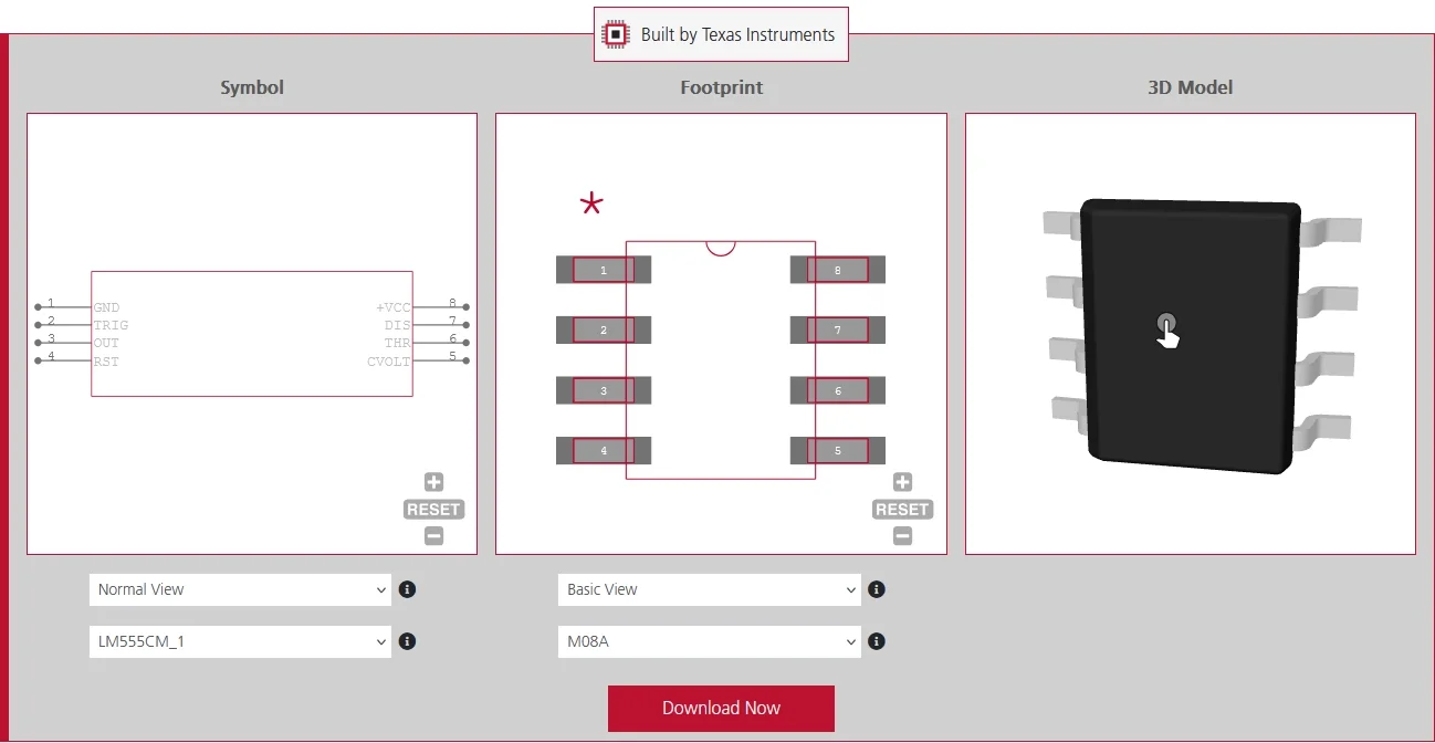
If you are looking for verified CAD models for the NE555, LM555, or CMOS variants, Ultra Librarian helps by compiling all your sourcing and CAD information in one place. Our platform provides verified, ready-to-use footprints, symbols, and 3D models that support all popular ECAD applications, along with sourcing information from worldwide distributors.
Working with Ultra Librarian sets your team up for success, ensuring streamlined and error-free design, production, and sourcing. Register today for free.