
For component manufacturers, getting a new part designed into a customer’s product is the ultimate goal. However, an often-overlooked bottleneck in the modern engineering workflow is the availability of accurate CAD models. If an engineer has to spend hours manually translating your datasheet into a physical land pattern, they are significantly more likely to choose a competitor’s part that comes with ready-to-use digital assets.
To remove this friction, industry leaders rely on verified PCB footprint programs. By providing engineers with guaranteed, high-quality schematic symbols, PCB footprints, and 3D models, manufacturers can accelerate design-ins, ensure Design for Manufacturability (DFM), and drastically reduce technical support requests. Here is how Ultra Librarian builds, verifies, and distributes the digital twins of your physical components.
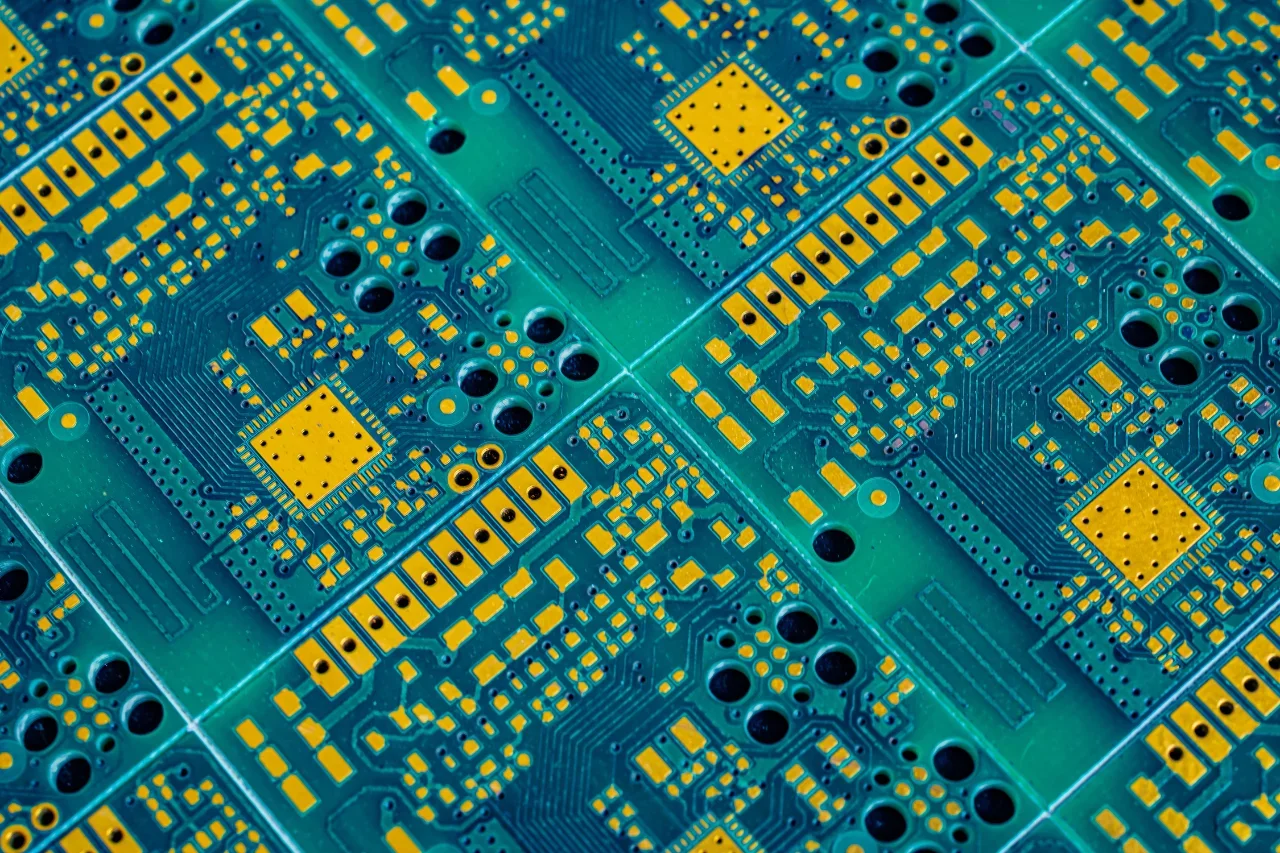
The High Cost of Manual Library Creation
In the ECAD environment, the PCB footprint library acts as the foundational bridge between electrical intent and physical reality. Historically, engineers created these footprints manually, a tedious, error-prone process. A single miscalculated pad dimension, an inverted polarity marker, or an incorrect courtyard can lead to catastrophic manufacturing failures. These issues manifest as solder bridging, tombstoning, or physical clearance collisions, ultimately leading to expensive board respins and delayed product launches.
When manufacturers participate in Verified PCB Footprint Programs, they eliminate this risk entirely for their customers, enabling component evaluation to lead to immediate implementation.
Standardized Library Structure
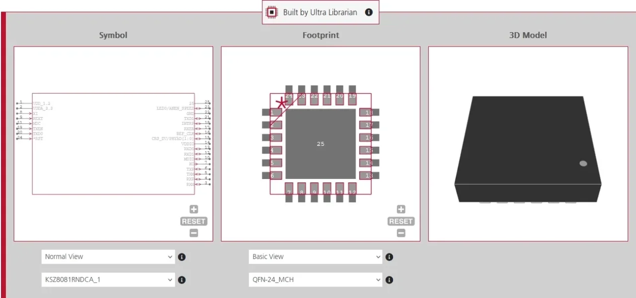
A true digital twin requires more than just a generic drawing. Ultra Librarian ensures that every component is built as a complete, cohesive package.
- The “Matched Set”: Every download includes a strictly linked schematic symbol, PCB footprint, and 3D STEP model. This guarantees that pin 1 on the schematic perfectly matches pad 1 on the physical board and the 3D enclosure.
- IPC Standards Compliance: Our models are built strictly to IPC-7351 standards (and evolving IPC guidelines) to ensure optimal solder joint reliability.
- Consistent Layer Conventions: We use standardized mechanical, silkscreen, and assembly layer conventions so your components drop seamlessly into any designer’s existing corporate library without requiring manual cleanup.
Verified PCB Footprint Programs
Trust between stakeholders is key in electronic design. To earn that trust, our verified PCB footprint programs utilize a rigorous, multi-tiered verification workflow.
- Datasheet-Driven Creation: Every dimension is extracted directly from the manufacturer’s official mechanical drawings and recommended land patterns.
- Automated & Manual Rule Checks: We run comprehensive rule checks on every asset before it reaches the engineer. This includes verifying:
- Pad Stacks: Exact sizing, drill holes, and tolerances.
- Polarity: Clear, unambiguous pin 1 and cathode markings on both silkscreen and assembly layers.
- Clearances: Pin-to-pin spacing to prevent solder webbing.
- Mask & Paste: Precise solder mask expansion and solder paste stencil definitions for optimal reflow.
- Courtyards: Accurate placement of courtyards to prevent physical collisions during automated assembly.
Rich Data and Native ECAD Integration
A geometric shape is useless without the intelligence behind it. We embed rich part metadata and parametrics directly into the CAD models, including Manufacturer Part Numbers (MPNs), descriptions, component heights, and datasheet links.
Furthermore, Ultra Librarian utilizes proprietary automated generators to export models into over 30 native ECAD formats, including Cadence (OrCAD/Allegro), Altium, Siemens (Mentor), and KiCad. Your customers get a native library file that behaves exactly as if they had built it themselves in their own software.
The Manufacturer Value: Quality, Yield, and Design-Wins
Investing in a verified CAD model strategy delivers immediate, measurable ROI for component manufacturers.
- Faster Design-Ins: By removing the hours required for manual library creation, you lower the barrier to entry for your components. Engineers download, place, and route.
- Fewer Support Issues: DFM-driven footprints mean fewer customers contacting your FAEs (Field Application Engineers) with questions about pad layouts, thermal relief, or soldering issues.
- Improved Customer Yield: When your customers use IPC-verified footprints, their manufacturing yields increase. Their success becomes tied to your components.
- Brand Trust: Providing a flawless digital experience reinforces your reputation as a premium, reliable manufacturer.
Manual Creation vs. Verified Programs
| Metric / Impact Area | Traditional Workflow (Manual Creation) | Ultra Librarian Verified Program |
| Time-to-Design-In | Hours to days (delayed by footprint creation). | Instantaneous (download and place). |
| Risk of Board Re-Spins | High (human error in pad sizing, polarity, etc.). | Near Zero (IPC-compliant, automated rule checks). |
| ECAD Compatibility | Generic formats requiring manual translation. | Native Support for 30+ major ECAD platforms. |
| FAE Support Burden | High (frequent customer questions on land patterns and mating). | Low (customers use guaranteed, ready-made assets). |
| Customer Experience | High friction; engineers may opt for a competitor’s part with existing models. | Seamless removes barriers to entry and builds brand loyalty. |
Don’t let missing or inaccurate CAD data cost you your next major design-win. Ensure your components are the easiest choice for engineers around the world. By joining Ultra Librarian’s verified PCB footprint programs, you place your entire product portfolio directly into the hands of the millions of engineers using our platform and our extensive distributor network.
Working with Ultra Librarian sets your team up for success, ensuring streamlined and error-free design, production, and sourcing. Contact UltraLibrarian for partnership opportunities.


")

