
Running out of General Purpose Input/Output (GPIO) pins is a rite of passage for any electronics designer. Whether you are building an LED matrix, driving multiple 7-segment displays, or controlling a bank of relays, microcontrollers have limits. The traditional and most cost-effective solution to this problem is the 74HC595—an 8-bit serial-in, parallel-out shift register.
By using just three pins on your microcontroller, the 74HC595 allows you to control eight separate outputs. Better yet, these chips can be daisy-chained to control 16, 32, or virtually an infinite number of digital outputs without using any additional microcontroller pins.
However, getting the timing right requires understanding the internal latches and clocks. By diving into the 74HC595 datasheet, designers can master the timing requirements and layout best practices needed to expand their I/O reliably. This guide breaks down the core specifications, operational timing, cascading techniques, and Arduino integration for the 74HC595.
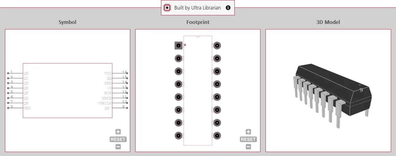
Decoding the 74HC595 Datasheet Pinout and Architecture
Before writing any code or routing a PCB, you must understand the pinout provided in the 74HC595 datasheet. While naming conventions sometimes vary slightly between manufacturers (e.g., Texas Instruments vs. Nexperia), the physical pin locations on the standard 16-pin package remain identical.
| Pin # | Common Name (TI / NXP) | Function | Description |
| 1-7, 15 | QA – QH (or Q0 – Q7) | Parallel Outputs | The 8 digital output pins. |
| 8 | GND | Ground | Ground connection (0V). |
| 9 | QH’ (or Q7S) | Serial Output | Outputs the data from the last stage of the shift register. Used for cascading to the next 74HC595. |
| 10 | SRCLR (or MR) | Shift Register Clear | Active-LOW. Pulling this low clears the internal shift register. Normally tied to VCC. |
| 11 | SRCLK (or SHCP) | Shift Register Clock | On the rising edge of this clock, data from the SER pin shifts into the register. |
| 12 | RCLK (or STCP) | Storage/Latch Clock | On the rising edge of this clock, data moves from the internal shift register to the actual output pins. |
| 13 | OE | Output Enable | Active-LOW. When HIGH, the outputs are put into a high-impedance (Hi-Z) state. Normally tied to GND to keep outputs active. |
| 14 | SER (or DS) | Serial Data Input | The pin where you feed the 1s and 0s from your microcontroller. |
| 16 | VCC | Power Supply | Typically operates between 2V and 6V. |
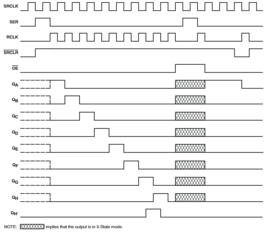
How It Works: Timing Diagram and Operation
The brilliance of the 74HC595 lies in its dual-register architecture: it has an internal Shift Register and a separate Storage Register (Latch). This ensures that the output pins do not flicker or change states while new data is being clocked in. The outputs only update when you explicitly tell them to.
The 3-Step Operation Process:
- Input Data: Apply a logic HIGH (1) or LOW (0) to the SER (Serial Data) pin.
- Shift it in: Send a single pulse (LOW to HIGH) to the SRCLK (Shift Register Clock) pin. This moves the data on the SER pin into the first bit of the internal shift register. Any data already in the register shifts over one spot. (Repeat steps 1 and 2 eight times to load a full byte).
- Latch to Output: Send a single pulse (LOW to HIGH) to the RCLK (Latch Clock) pin. This copies the 8 bits from the internal shift register directly to the output pins (Q0-Q7) simultaneously.
Common Applications of 74HC595
Because of its simplicity and low cost, the 74HC595 is ubiquitous in digital design. Common applications include:
- GPIO Expansion: Adding extra digital outputs to constrained microcontrollers (like an ESP32 or basic Arduino) for controlling relays, optocouplers, or status LEDs.
- 7-Segment Displays: A single 74HC595 perfectly matches the 8 connections needed for a 7-segment display (seven segments plus the decimal point). By cascading them, you can easily drive multi-digit displays.
- LED Matrices and Chasers: Used in combination with a decade counter or a row-driver, shift registers are the standard way to control the columns of large LED dot-matrix displays, clocking out patterns at high speeds.
Interfacing with Microcontrollers: Hardware SPI and Libraries
While many beginners learn to use the 74HC595 by “bit-banging” pins via software, professional designs require faster approaches.
1. Hardware SPI for High Speed:
For applications such as LED matrices, where display refresh rates are critical, software bit-banging is too slow. Instead, connect the 74HC595 to the microcontroller’s hardware SPI pins:
- Connect MOSI to the SER (Data) pin.
- Connect SCK to the SRCLK (Shift Clock) pin.
- Use any digital GPIO pin for RCLK (Latch).
Using hardware SPI allows you to push data to the shift register at MHz speeds, utilizing dedicated microcontroller hardware rather than consuming CPU clock cycles.
2. Recommended Libraries (Arduino Ecosystem):
For complex projects with multiple cascaded chips, managing the bitwise math manually becomes tedious. Using community-vetted libraries significantly speeds up development:
- ShiftRegister74HC595 (by Timo Denk): This is highly recommended for Arduino and compatible environments. It allows you to treat the output pins of the shift register as if they were virtual microcontroller pins. You can easily set individual pins HIGH or LOW without having to manually reconstruct and shift the entire byte structure.
Cascading Multiple 74HC595 ICs
To control 16, 24, or 32+ outputs, you can daisy-chain multiple 74HC595 chips together.
The Hardware Circuit:
- Connect the QH’ (Pin 9) of the first 74HC595 to the SER (Pin 14) of the second 74HC595.
- Tie all the SRCLK (Clock) pins together to the same microcontroller clock pin.
- Tie all the RCLK (Latch) pins together to the same microcontroller latch pin.
The Cascading Data Flow
When cascading, data acts like water in a pipe. The first 8 bits you send will overflow from the first chip’s QH’ (Serial Out) pin and slide directly into the SER (Serial In) pin of the second chip. To update all 16 (or more) outputs simultaneously, you must pull the shared latch pin LOW, shift out all the necessary bytes for every chip in the chain, and then pull the latch pin HIGH. This updates all outputs at the exact same moment without any visible flickering.
Comparing Alternatives: 74HC164 and TPIC6B595
Depending on your specific load and timing requirements, the 74HC595 might not be the perfect fit. Consider these alternatives:
- 74HC164 (No Latch): This is a simpler 8-bit shift register without an output storage latch. As you clock data in, the output pins update immediately and visibly ripple. It is generally avoided for driving LEDs or relays where intermediate “flickering” states cause problems, but it is useful for specific data-routing scenarios.
- TPIC6B595 (High Current): The standard 74HC595 can source/sink about 35mA per pin, but has a strict thermal limit of ~70mA total for the entire chip. If you try to turn on 8 LEDs at 20mA each, the standard chip will overheat. The TPIC6B595 is the heavy-duty alternative. It features open-drain power MOSFET outputs capable of sinking 500mA per channel, making it ideal for driving high-power LEDs, motors, or solenoids.
PCB Layout Guidelines for High-Speed Operation
According to the 74HC595 datasheet, these ICs can handle clock frequencies up to 100 MHz (at 5V VCC). At these speeds, PCB layout becomes critical to prevent data corruption.
- Decoupling is Mandatory: Place a 0.1µF ceramic decoupling capacitor as physically close as possible to the VCC (Pin 16) and GND (Pin 8) pins of every shift register in the chain. This provides a local energy reservoir during the high-speed switching of 8 simultaneous outputs, preventing voltage droop and logic resets.
- Trace Routing: When cascading multiple chips, the shared SRCLK and RCLK lines can become quite long, acting as antennas. Keep these traces as short and direct as possible. Avoid routing them parallel to noisy power lines or analog traces to prevent crosstalk and false clock triggers.
- Signal Integrity: If driving multiple cascaded chips at high speeds, the capacitance on the shared clock lines increases significantly. You may need to add a small series damping resistor (e.g., 33Ω to 47Ω) near the microcontroller’s clock output to reduce ringing and EMI reflections on the line.
If you need accurate CAD models that reflect the exact physical specifications in the 74HC595 datasheet, Ultra Librarian compiles all your sourcing and CAD information in one place.
Our platform provides verified, IPC-compliant footprints, symbols, and 3D models for the 74HC595 supporting all package types (SOIC, TSSOP, and DIP) for all popular ECAD applications, alongside real-time sourcing information from worldwide distributors.
Working with Ultra Librarian sets your team up for success, ensuring streamlined and error-free design, production, and sourcing. Register today for free.


")

