Field Programmable Gate Arrays (FPGAs) are the “Swiss Army knives” of the electronics world. Unlike traditional microcontrollers, which execute sequential instructions in software, FPGAs can be reconfigured at the hardware level to implement custom digital logic. This allows designers to tailor the architecture to a specific application, enabling high parallelism and, in many cases, significantly better performance and lower latency.
While FPGAs offer greater hardware flexibility, they also come with higher cost, power consumption, and design complexity. Choosing the wrong FPGAs can lead to unnecessary expense, inefficiency, or insufficient resources. This FPGA selection guide breaks down the technical variables you need to consider to pick the best device for your project.
Understanding the Core Hardware Variables
Before looking at specific brands, you must define the “size” of the chip you need. FPGAs are measured by several key internal resources.
Logic Capacity (LUTs)
At the most basic level, FPGAs implement digital circuits using logic gates (such as AND, OR, and XOR). The primary building block for this logic is the Look-Up Table (LUT), which stores truth tables to implement combinational logic functions. In other words, this is where your digital logic is actually realized on the device. Manufacturers group LUTs together with other resources (such as flip-flops) into larger units called Logic Elements (LEs) or Logic Cells (LCs), depending on the vendor.
While some designs start with FPGAs for high-performance needs, many begin with microcontrollers due to their simplicity and lower cost, then transition as requirements outgrow their capabilities. These capabilities include performance limits, the need for true parallelism or low latency, higher I/O requirements, strict real-time constraints, or custom digital interfaces. In some cases, an FPGA can also consolidate multiple components into a single device.
If you are moving a design from a microcontroller, estimating logic requirements can be challenging because you are transitioning from a fixed, sequential processor to a fully customizable hardware architecture. A good rule of thumb is to look at reference designs for similar tasks (like image processing or motor control) and add a 30% buffer to account for design growth.
I/O Count and Standards
FPGAs are often selected when a design needs to interface with many signals simultaneously without performance loss, for example, controlling multiple sensors, memory devices, or parallel data buses. To ensure these connections operate reliably, it’s important to understand the supported I/O standards:
- CMOS/TTL: Used for general-purpose, lower-speed digital signals (e.g., buttons, LEDs, simple peripherals).
- LVDS (Low-Voltage Differential Signaling): Used for high-speed, low-noise communication over longer distances (e.g., displays, high-speed data links).
For even higher data rates, standard I/O is not sufficient. Dedicated transceivers or SERDES (Serializer/Deserializer) blocks are required. These hardware blocks convert parallel data into high-speed serial streams (and back again on reception), allowing reliable communication at gigabit speeds. They are essential for protocols like PCIe or 10Gb Ethernet, where traditional GPIO or LVDS-based I/O cannot support the required bandwidth or signal integrity.
Speed (Clocking and Data Rate Capability)
FPGA “speed” is not just a single number; it is determined by multiple factors:
- Logic switching speed (fabric clock rate): how fast internal LUT-based logic can operate
- Timing closure capability: how reliably the design can meet timing at higher frequencies
- DSP and memory clock rates: often higher optimized speeds than general logic
- Transceiver data rate (critical factor): typically ranges from ~1 Gbps in mid-range devices to 112+ Gbps in high-end FPGAs
In practice:
- Low-power FPGAs: tens to ~200 MHz fabric clocks
- Mid-range: ~200–600 MHz (design-dependent)
- High-end: optimized paths + transceivers enable multi-GHz serial communication
This is why high-speed systems rely on SERDES rather than parallel GPIO. Parallel buses cannot scale cleanly at very high frequencies due to skew and signal integrity issues.
Memory and DSP Slices
Most FPGAs include internal random-access memory (RAM) and dedicated Digital Signal Processing (DSP) slices, which are specialized hardwired processing blocks built into the FPGA fabric. DSP slices are optimized for high-speed mathematical operations such as multipliers and multiply-accumulate (MAC) functions, making them ideal for workloads like FFTs, filtering, and other signal processing tasks.
If your design involves heavy computation, you’ll want an FPGA with sufficient DSP slice count to handle the workload efficiently. Likewise, if you are buffering large amounts of data, ensure the chip has enough internal RAM or supports external memory interfaces such as DDR4 or DDR5.
Package Type (Physical Constraints)
The FPGA package defines how the silicon connects to the outside world and directly affects routing, cost, and manufacturability.
Common package types include:
- QFP (Quad Flat Package):
~100–256 pins, easy to solder, used in low-end and prototyping designs - BGA (Ball Grid Array):
~256–2000+ pins, standard for mid/high-end FPGAs, requires PCB vias and more complex assembly - FCBGA / Flip-chip BGA:
Used in high-performance devices; supports very high pin counts and high-speed routing
FPGA Selection Guide Steps
FPGA is typically discussed in tiers: low-power, mid-range, and high-performance, but these are informal groupings rather than strict categories. In general, as you move up these tiers, costs increase due to more logic resources, higher performance capabilities, and additional specialized hardware blocks.
Match the FPGA Family to the Application
Manufacturers typically divide their products into three tiers:
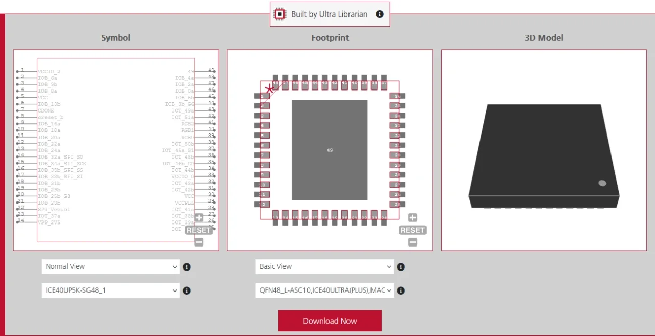
Low-Power/Small Form Factor: FPGAs like Lattice iCE40 or Intel Cyclone are meant for simple I/O expansion, handheld devices, and basic sensor fusion. These are typically used when cost, size, and power efficiency matter more than raw performance. They are also commonly chosen as “helper chips” alongside a microcontroller.
Mid-Range: FPGAs like the Xilinx Artix or Intel Arria offer significantly more logic, better I/O capabilities, and often include SERDES/transceivers and moderate DSP/memory resources. Used in industrial control, embedded vision, communications, and mid-level signal processing. These devices are often selected when real-time processing or parallel computation becomes necessary. They provide a balance between performance and system complexity, making them the most widely used class in industrial applications.
High-Performance: The Xilinx Virtex or Intel Stratix series are behemoths designed for data centers, radar systems, and 5G infrastructure. They provide massive logic capacity but require complex cooling and power systems. These FPGAs are used in extremely data-intensive systems where throughput and parallelism are critical. They are often treated as hardware accelerators rather than traditional embedded components.
Evaluate the Toolchain
You are not just buying a chip; you are committing to a toolchain – the complete software environment used to design, simulate, synthesize, and program the FPGA. Most high-end FPGAs require proprietary software suites like AMD Vivado or Intel Quartus. Check if the software is free for the device you are picking. Some enterprise-level chips require expensive annual licenses just to compile the code.
Assess Development Risk and Availability
Choose FPGAs with strong long-term availability commitments, meaning the manufacturer guarantees the FPGA will continue to be produced and supported for many years. This is important because industrial and commercial products often have a 10–15-year lifecycle, and replacing hardware mid-production can be costly and disruptive.
Furthermore, check for existing IP cores (pre-written code blocks). For example, if you need to implement a USB 3.0 interface, selecting an FPGA with a verified IP core will save you months of work.
Common FPGA Selection Mistakes
Many FPGA selection issues come from underestimating system requirements early in the design process. A device may appear sufficient initially, but can fail under real-world workloads, interface constraints, or lifecycle constraints.
- Underestimating overall resource requirements: Designers often select an FPGA based on early prototypes without enough headroom in LUTs, DSP slices, or memory, which can limit scalability as features are added later.
- Ignoring I/O, speed, and interface constraints: Choosing a device without sufficient pin count, correct I/O standards, or SERDES support can prevent proper integration with sensors, memory, or high-speed communication protocols.
- Overlooking system-level constraints: Power consumption, thermal design requirements, toolchain complexity, and long-term device availability are often underestimated, leading to integration or production challenges.
- Cost-driven or inefficient architectural decisions: Selecting the cheapest FPGA or rebuilding standard functionality rather than using proven IP cores can increase development time, risk, and long-term system costs.
Low-Power vs. High-Performance FPGA Comparison
| Feature | Low-Power | Mid-Range | High-Performance |
| Logic Density | 1k – 150k LCs | 50k – 500k LCs | 500k – 5M+ LCs |
| Power Consumption | Milliwatts | 1W – 10W | 10W – 100W+ |
| Cooling Need | Usually none | A passive heatsink sometimes | Heatsinks / Active fans |
| Price Point per chip | $2 – $50 | $50 – $500 | $500 – $10,000+ |
| Common Uses | IoT devices, Glue Logic, Mobile devices | Embedded systems, industrial control, and machine vision | Networking, AI, Aerospace, Defense |
| Example FPGA Chips | Lattice iCE40 (UltraPlus, HX) | Xilinx Artix-7, Intel Cyclone V | AMD Virtex-7, Virtex UltraScale+ |