The TL431 is an industry-standard component used in almost every switch-mode power supply for isolated voltage feedback. Power supply designers use a TL431 adjustable precision shunt regulator datasheet to calculate reference voltages and maintain adequate phase margin. The document provides the exact tolerances and boundary conditions needed for safe hardware operation. Such technical documentation also outlines how the three-terminal device functions as an adjustable Zener diode.
- A conventional Zener diode provides a fixed voltage drop through passive breakdown. Diodes rated below roughly 5 V break down via quantum tunneling, while those rated above 5 V rely on avalanche breakdown.
- The TL431 provides a variable voltage drop ranging from 2.495 V to 36 V via internal circuitry.
The internal error amplifier compares the voltage at the Reference pin against an internal 2.495 V bandgap reference. When the Reference pin voltage exceeds the bandgap reference, the error amplifier turns on an internal bipolar transistor. Consequently, the transistor sinks current from the Cathode pin to the Anode pin. This active feedback mechanism gives the component a significantly sharper turn-on characteristic than a standard Zener diode.
Navigating the TL431 Adjustable Precision Shunt Regulator Datasheet
The TL431 adjustable precision shunt regulator datasheet contains multiple sections detailing electrical characteristics and physical dimensions. Engineers typically look first at the absolute maximum ratings table. The ratings define the physical limits of the component, such as a maximum cathode voltage of 37 V and a maximum continuous cathode current of 150 mA.
Operating the part beyond the absolute maximums will cause permanent damage. Recommended operating conditions provide a narrower, safer range for daily operation. For example, manufacturers recommend maintaining a minimum cathode current of 1 mA to keep the internal error amplifier actively regulating.
Absolute maximum ratings from the TL431 Datasheet
| Symbol | Parameter | Value | Unit |
| VKA | Cathode to anode voltage | 37 | V |
| Ik | Continuous cathode current range | -100 to +150 | mA |
| Iref | Reference input current range | -0.05 to +10 | mA |
| Rthjc | Thermal resistance junction to case TO-92 SO-8 batwing SOT23-3L SOT23-5L SOT323-6L | 57 30 136 67 110 | °C/W |
| Rthja | Thermal resistance junction to ambient TO-92 SO-8 batwing SOT23-3L SOT23-5L SOT323-6L | 200 85 248 157 221 | °C/W |
| Tstg | Storage temperature range | -65 to +150 | °C |
| TJ | Junction temperature | 150 | °C |
| Electrostatic Discharge | TL431IY, TL431AIY-T: HBM (human body model)(1) TL431-TL432: HBM (human body model) MM: machine model(2) CDM: charged device model(3) | 3000 2000 200 1500 | V |
Pin Configuration and Common Packages
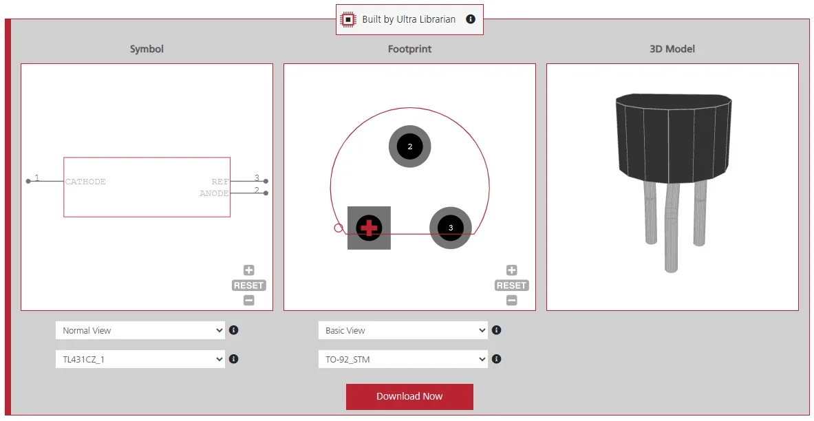
Pinout orientation leads to frequent design errors in printed circuit board layout. For example, reversing the Anode pin and Cathode pin is a common mistake preventing the error amplifier from regulating the voltage.
This kind of error becomes more likely when a schematic symbol and its matching PCB footprint are built separately by hand, since a pin swapped in one model but not the other won’t surface until board bring-up. Sourcing a pre-verified TL431 model removes the risk before layout even begins. The three standard pins are:
- Reference: Receives the feedback signal from a resistor network.
- Anode: Connects directly to the circuit ground.
- Cathode: Connects to the power supply output through a current-limiting resistor.
Manufacturers package the TL431 component in several physical form factors to accommodate varying power-dissipation requirements. The next table outlines the most common physical packages.
Common TL431 Packages and Dimensions
| Package Type | Pin Count | Typical Body Size (mm) | Common Application |
| SOT-23-3 | 3 | 2.90 x 1.30 | High-density PCBs |
| SOIC-8 | 8 | 4.90 x 3.90 | General surface mount |
| TO-92 | 3 | 4.30 x 4.30 | Through-hole designs |
| SOT-89 | 3 | 4.50 x 2.50 | High-dissipation layouts |
The SOIC-8 package contains several unconnected internal pins. Designers should leave the extra pins floating or tied to the ground, depending on the specific manufacturer guidelines. Note: different manufacturers produce functionally identical components with slight package variations. As a result, cross-referencing the specific mechanical drawings prevents footprint mismatch.
Calculating the Output Voltage
The output voltage depends directly on a resistive voltage divider connected to the component. The designer connects two external resistors to the reference pin, with the upper resistor attached to the cathode pin and the lower resistor attached to the anode pin. The internal bandgap reference forces the error amplifier to hold the reference pin at a steady 2.495 V.
Calculating the output voltage requires basic algebra. The output voltage equals the internal reference voltage multiplied by one plus the ratio of the two external resistors, plus a small error factor. The exact equation is:

The reference input current (Iref) is typically around 2 microamps. Such a low current value means the Iref term has a negligible effect when using resistor values under 10 kilohms.The reference input current (Iref) is typically around 2 microamps. Such a low current value means the Iref term has a negligible effect when using resistor values under 10 kilohms.The reference input current (Iref) is typically around 2 microamps. Such a low current value means the Iref term has a negligible effect when using resistor values under 10 kilohms.
On resistor tolerance:
- The resistor tolerance directly affects the final output accuracy.
- Using 1% or 0.1% tolerance resistors for the voltage divider limits initial output error.
- If the resistors drift with temperature changes, the output voltage will change, even though the internal TL431 bandgap reference remains highly stable.
Standard carbon film resistors introduce unnecessary thermal variance. Instead, metal film resistors provide a stable divider network for the Reference pin.
Optocoupler Integration for Isolated Feedback
Isolated power supplies require a physical barrier between the primary and secondary sides. Engineers pair the TL431 with an optocoupler to safely cross the isolation boundary. The Cathode pin connects directly to the light-emitting diode (LED) inside the optocoupler. When the secondary voltage rises, the component draws more current through the Cathode pin, which brightens the optocoupler LED.
The phototransistor on the primary side detects the light and signals the switching controller to adjust its pulse width. The sharp response of the error amplifier makes the feedback mechanism highly responsive to sudden load changes. A dedicated pull-up resistor ensures the component always receives a minimum operating current of 1 mA, even at minimum load. As a result, the error amplifier stays within its linear regulation range rather than dropping out.
Addressing Loop Stability and Boundary Conditions
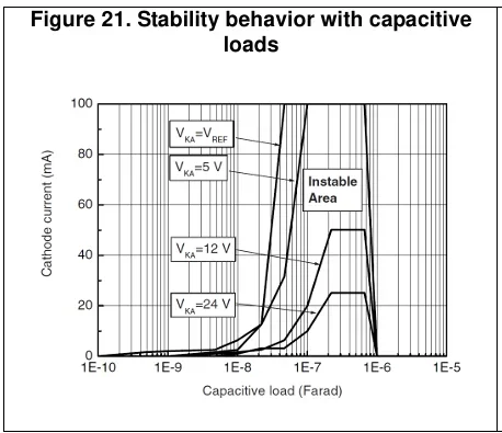
Power supply control loops frequently suffer from unwanted oscillation. The stability boundary conditions chart is a graph in the technical documentation. The chart plots load capacitance against cathode current to identify the regions where the feedback loop remains stable. The TL431 has specific regions of instability where internal error amplifier ringing or oscillation leads to erratic power-supply behavior designers must avoid.
Managing phase margin:
- Engineers should choose load capacitors carefully to maintain phase margin.
- A capacitor placed directly across the Anode pin and Cathode pin creates a pole in the control loop transfer function.
- If the equivalent series resistance (ESR) of the capacitor is too low, the phase margin drops below zero.
- Adding a small discrete series resistor to the capacitor often restores the lost phase margin.
- Accordingly, the stability boundary conditions chart shows exactly which capacitance values to avoid for a given cathode current.
Dynamic Impedance and Frequency Response
Dynamic impedance indicates how well the component rejects unwanted current variations. A perfect Zener diode would have zero dynamic impedance. The TL431 boasts a typical dynamic impedance of 0.22 ohms. Such a low impedance means a large change in cathode current results in only a tiny change in cathode voltage. The active internal circuitry maintains tighter regulation than the passive avalanche breakdown mechanism in a standard Zener diode.
Frequency response:
- The Bode plot shows the open-loop voltage gain of the internal error amplifier.
- The open-loop gain is typically around 50-60 dB at low frequencies.
- The gain rolls off as the operating frequency increases.
- The unity-gain crossover frequency usually sits near 1 MHz.
- Engineers use the Bode plot to design compensation networks.
A compensation capacitor placed between the Reference pin and Cathode pin shapes the frequency response. The capacitor prevents the power supply control loop from ringing during sudden load transients.
Temperature Grades and Thermal Drift
Temperature fluctuations affect internal semiconductor behavior. The manufacturer categorizes the component into distinct temperature grades based on thermal testing. The standard commercial grade operates from 0 to 70 degrees Celsius. Industrial and automotive grades significantly extend the operating range in harsher environments. Advantageously, the internal voltage deviation over the entire temperature range typically stays below 10 millivolts.
Typical TL431 Temperature Grades
| Suffix | Grade Level | Operating Temperature Range |
| C | Commercial | 0 °C to 70 °C |
| I | Industrial | -40 °C to 85 °C |
| Q | Automotive | -40 °C to 125 °C |
| M | Military | -55 °C to 125 °C |
Initial voltage tolerance separates the various part numbers in the TL431 family. The specific precision options include:
- Standard Grade: Offers a 2% initial tolerance at 25 degrees Celsius.
- A-Grade: Tighter tolerance sits at 1%.
- B-Grade: Offers the tightest precision at 0.5% initial tolerance.
Power supply designers select the exact grade based on the target application’s overall error budget. High-precision laboratory equipment requires the B-grade part to maintain strict output accuracy. Consumer electronics often rely on standard-grade components to reduce manufacturing costs.
The TL431 is an electronic engineering staple because the device offers predictable, highly accurate voltage regulation. Reviewing the component specifications ensures a new circuit design stays within safe thermal limits and stability boundaries. Building this TL431 model by hand across schematic, layout, and simulation tools can take hours of manual copy-and-paste, and a single mismatch in pin count or footprint dimensions among those models can lead to a costly respin.
Locating a verified TL431 adjustable precision shunt regulator datasheet is easy with Ultra Librarian, which provides accurate schematic symbols, PCB footprints, and 3D models for popular ECAD applications. Search for specific electronic parts and connect with worldwide distributors to source components instantly.
Working with Ultra Librarian sets your team up for success, ensuring streamlined and error-free design, production, and sourcing. Register today for free.

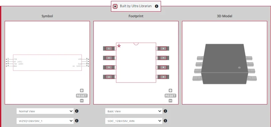

 If you’re looking for any of our component footprints or models, we have readily available and free options for you and your design team. Search our library for the solution you’ve been looking for.