The rapid proliferation of Internet of Things (IoT) devices generates massive amounts of data requiring reliable external storage. Because modern microcontrollers lack sufficient internal memory for over-the-air (OTA) updates and data logging, engineers frequently utilize external SPI flash devices. The W25Q128 serial flash memory datasheet provides the exact specifications needed to integrate this popular 128M-bit non-volatile storage chip.
By understanding the communication protocols, read and write speeds, and low-power modes detailed in the documentation, hardware designers can optimize storage solutions for space-constrained embedded systems.
SPI Protocols in the W25Q128 Serial Flash Memory
The W25Q128 operates using the Serial Peripheral Interface (SPI). To maximize data throughput while minimizing pin count on the Printed Circuit Board (PCB), the device supports three distinct communication modes:
- Standard SPI: Utilizes a standard four-wire interface consisting of Clock (CLK), Chip Select (/CS), Data In (DI), and Data Out (DO).
- Dual SPI: Converts the DI and DO pins into bidirectional I/O pins (IO0 and IO1), doubling the data transfer rate per clock cycle.
- Quad SPI: Repurposes the Write Protect (/WP) and Hold (/HOLD) pins into additional data lines (IO2 and IO3). Such a configuration allows four bits of data to transfer simultaneously.
Consequently, Quad SPI provides exceptional performance for systems executing code directly from external memory, known as eXecute In Place (XIP).
Pin Configuration and Electrical Limits
The memory chip is commonly manufactured in 8-pin SOIC (Small Outline Integrated Circuit) and WSON (Very Very Thin Small Outline No-Lead) packages. Both physical formats share an identical pinout logic to simplify PCB routing.
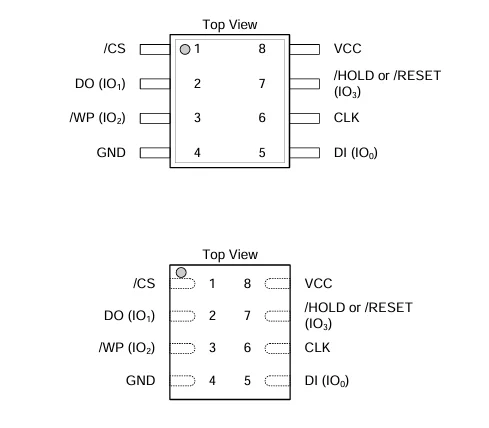
W25Q128 Standard 8-Pin Configuration
| Pin Number | Pin Name | Standard SPI Function | Quad SPI Function |
| 1 | /CS | Chip Select (Active Low) | Chip Select |
| 2 | DO / IO1 | Data Output | Bidirectional Data 1 |
| 3 | /WP / IO2 | Write Protect | Bidirectional Data 2 |
| 4 | GND | System Ground | System Ground |
| 5 | DI / IO0 | Data Input | Bidirectional Data 0 |
| 6 | CLK | Serial Clock | Serial Clock |
| 7 | /HOLD / IO3 | Hold or Reset Input | Bidirectional Data 3 |
| 8 | VCC | Power Supply | Power Supply |
Electrical Design Considerations
Beyond physical connections, hardware engineers must design the W25Q128 circuit within its specified electrical limits. Exceeding absolute maximum ratings can cause permanent silicon damage, reduced reliability, or device failure. Key considerations include:
- Operating Voltage: The W25Q128 requires a 2.7 V to 3.6 V supply range. Stable power regulation is critical to prevent unreliable read/write operations or component damage.
- Temperature Rating: Industrial-grade variants support operation from -40 °C to +85 °C, making thermal management important for systems exposed to harsh environments.
- Input/Output Protection: Transient voltages exceeding VCC + 0.5 V on any I/O pin can cause latch-up or immediate failure. Voltage translation, clamping, and proper interface protection should be considered for mixed-voltage designs.
- Power Integrity: High-speed SPI communication creates rapid current changes. Therefore, low-ESR (Equivalent Series Resistance) ceramic decoupling capacitors placed close to the VCC pin help reduce supply noise and maintain stable operation.
- Signal Integrity: At higher SPI clock speeds, ringing and overshoot on CLK and data lines can cause communication errors. Controlled impedance routing, short traces, and proper termination techniques help maintain reliable data transfer.
W25Q128 Serial Flash Memory Datasheet Performance Metrics
Performance metrics are a primary focus for hardware engineers reviewing the W25Q128 serial flash memory datasheet. The device supports high clock frequencies to facilitate rapid data retrieval and storage. In Standard SPI mode, the clock frequency reaches up to 133 MHz. When using Quad SPI, the simultaneous four-bit transfer yields an equivalent data transfer rate of 532 Mbit/s (133 MHz clock × 4 data lines), while the clock frequency itself remains 133 MHz.
W25Q128 SPI Communication Modes and Transfer Rates
| SPI Mode | Active Data Pins | Max Clock Frequency | Equivalent Transfer Rate |
| Standard SPI | 1 (DI/DO) | 133 MHz | 133 Mbits/s |
| Dual SPI | 2 (IO0, IO1) | 133 MHz | 266 Mbits/s |
| Quad SPI | 4 (IO0, IO1, IO2, IO3) | 133 MHz | 532 Mbits/s |
Furthermore, high transfer speeds allow fast booting times and rapid firmware updates. Page programming typically takes 0.7 milliseconds. Erase operations take longer and scale with the size of the memory block:
- A 4 KB sector erase typically takes 45 ms (400 ms max).
- A 64 KB block erase typically takes 150 ms (2,000 ms max).
- A full chip erase typically takes 40 seconds (200 seconds max).
Architecture and Sector Organization
The 128M-bit array is organized into uniform, erasable segments. Such architecture simplifies firmware wear-leveling algorithms. The total memory is divided into:
- 65,536 programmable pages of 256 bytes each.
- 4,096 erasable sectors of 4 Kilobytes (KB) each.
- 256 erasable blocks of 64 KB each.
The 4 KB sector erase capability provides high flexibility for data logging applications, allowing the microcontroller to erase small chunks of data without rewriting an entire 64 KB block.
Low-Power Operating Modes for IoT Devices
Battery-operated IoT sensors demand extreme energy efficiency. The datasheet outlines several power states designed to extend battery life.
- Active Mode: The chip draws approximately 15-25 mA during continuous read, program, or erase operations.
- Standby Mode: When the chip select pin is high, the device enters standby mode, reducing current consumption to approximately 10 µA.
- Power-Down Mode: Engineers can issue a specific software instruction to enter deep power-down. Such a state drops current consumption to a mere 1 µA.
Therefore, properly managing power states ensures the flash memory chip conserves energy when the host microcontroller sleeps.
Choosing the Right Flash Memory for Your Next Design
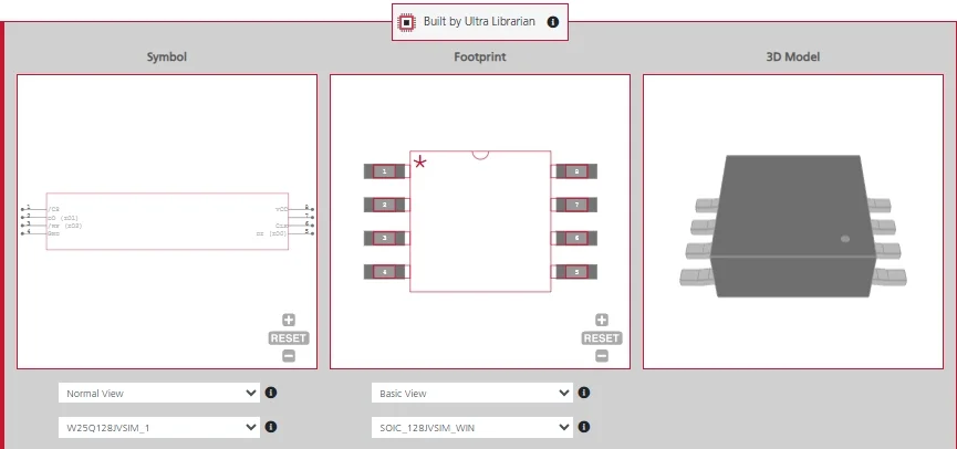
If you’re looking for Computer-Aided Design (CAD) models for common components or the W25Q128 serial flash memory datasheet, Ultra Librarian helps by compiling all your sourcing and CAD information in one place.
Working with Ultra Librarian sets your team up for success by ensuring streamlined, error-free design, production, and sourcing. Register today for free.



 If you’re looking for any of our component footprints or models, we have readily available and free options for you and your design team. Search our library for the solution you’ve been looking for.