

Basic PCB fabrication terminology starts with manufacturing files, as designers will need to generate these before sending their board in for quote. It’s also important to understand the bare-board fabrication process, as this aids DFM practices, design reviews, and communicating design intent.
FABRICATION FILE TERMINOLOGY
PCB fabricators will use multiple data files to prepare fabrication instructions and inspect a design. Most fabricators will not request a designer submit their design files in their ECAD application format. Instead, the PCB fabrication industry requires a set of standard file formats before they can start building a bare PCB. Here are the essential files needed to start PCB fabrication:
These vector image files are used with a photoplotter to generate stencils for fabricating each layer in a bare board. The common Gerber file formats are RS-274-X and X2 as defined by Umaco. The older Gerber file format RS-274-D is no longer supported.
Two vendor-neutral fabrication file formats used to generate fabrication stencils.
A file listing all connections between nodes in a schematic. This file is used to inspect Gerber files before creating stencils, and to develop procedures for continuity testing during assembly.
A fabricator will use Gerbers, ODB++, IPC-2158 files, and a netlist to inspect a design before placing it into fabrication. Fabricators will generally not look at the design files or at your component libraries.
A standard drawing showing how layers are arranged in the PCB stackup, the copper features in each layer, locations of drill hits in the bare board, and other stencil features in each layer. A fabrication drawing will also include a drill table and other fabrication notes needed to ensure quality and yield.
A data file containing the X-Y coordinates of drill holes, drill sizes, and tooling numbers. This file is sometimes called an Excellon drill file or an NC drill file.
A table showing all drill bit sizes and tolerances used to fabricate a board. A drill table will often list plated or non-plated drill holes in a design.
A stainless steel or aluminum stencil used to define circuit features. Stencils are used to define copper features for etching, and in PCB assembly for applying solder paste (called a “paste mask” in some ECAD software). Stencils are cut using a laser and may be attached to a frame.
Small adjustments made to copper features in Gerber files to compensate for overetching during PCB fabrication. The amount of etch compensation depends on the specific etchant, copper weight on the panel, and processing steps used during panel fabrication.
BARE BOARD AND PANEL TERMINOLOGY
Bare boards are produced from PCB panels, where multiple boards are placed on a large panel and fabricated in parallel. The entire PCB stackup is constructed for all boards at once, giving a high throughput fabrication process.
All layers in a PCB start as copper-clad laminates. Copper foil is bonded to an insulating dielectric, known as core or prepreg. The dielectric is normally a fiberglass weave impregnated with a resin.
Two versions of copper-clad laminates. Core layers are generally thicker and will form the main interior of the PCB, while the prepreg is used as the “glue” to bond cores and other prepreg layers together into a stackup.
Core and prepreg characteristics are described in slash sheets under IPC 4101 (rigid laminates) and IPC 4103 (flex laminates). These two standards were created to help ensure laminate interoperability.
Refers to the copper foil placed on the surfaces of copper-clad laminates.
A hydrocarbon-based adhesive material commonly used to build stackups in high frequency circuit boards.
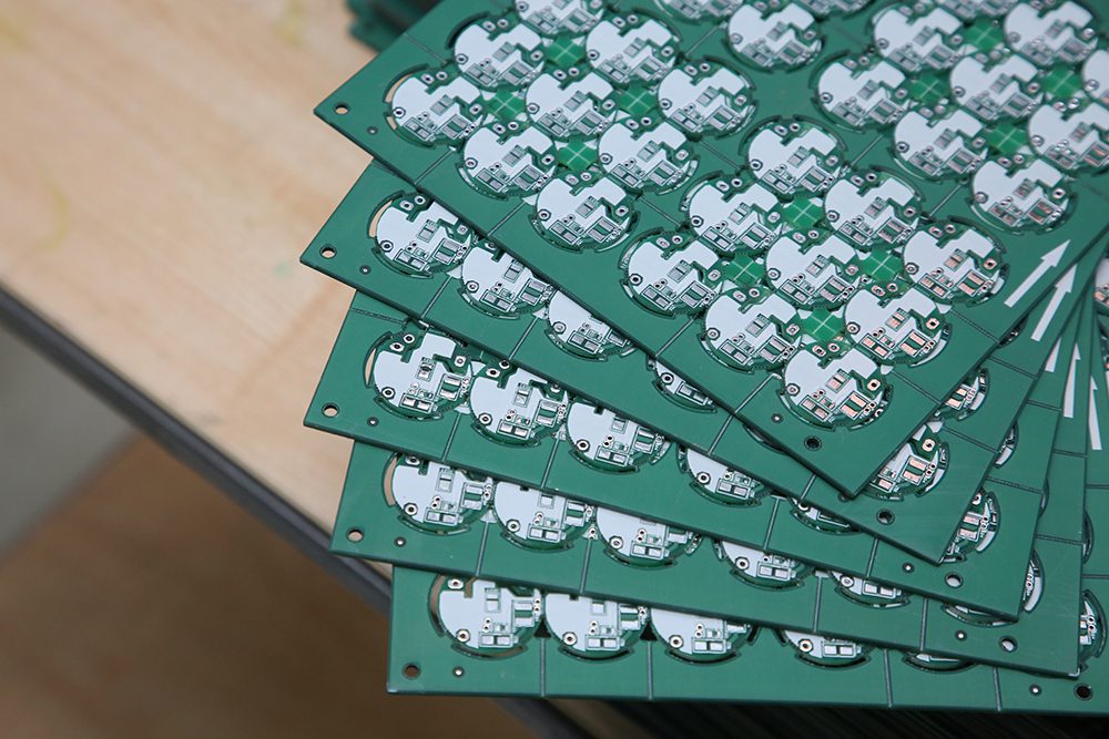
A layout of multiple copies of a circuit board in a single sheet of laminate material. PCB fabricators will etch, drill, and laminate an entire panel at once to increase throughput. The common panel size is 18” by 24”.
The process used to create the stackup in a production PCB panel. This involves heating and pressing layers together to force the resin in each layer to flow and bond, creating strong adhesion between layers.
Refers to the final hardened stage of resin used during the lamination process.
A method for placing grooves around boards in a PCB panel so they can be easily snapped out of the panel. Each copy of the PCB is held in place with breakaway tabs, which are small sections of the panel that can be snapped off.
Breakaway tabs are placed around the edges of these PCBs so they can be easily removed from the panel
A set of reference points used by automated fabrication and assembly equipment to determine the orientation of a board as it moves through the manufacturing process.
A set of precisely sized traces fabricated in the tooling area. These traces are used to test for controlled impedance during fabrication. Both differential and single-ended traces can be placed on a test coupon.
A test run of the fabrication process, followed by inspection. This is used to verify that the process does not produce excessive defects during fabrication.
PCB FABRICATION PROCESS TERMINOLOGY
There are several processes used to fabricate a bare board within a PCB panel. The PCB fabrication process begins by defining features on each layer with etching, followed by creating a stackup construction with pressing and etching. Drilling, milling, and plating processes are used to finish the bare board. Finally, a cleaning process makes the board ready for final inspection and assembly. Here are some of the key terms used throughout the fabrication process:
A process used to remove copper from a copper-clad laminate, leaving behind traces and pads on each layer of the PCB. This process uses an etchant solution (usually ferric chloride).
Fabricators will apply etch compensation to copper traces in fabrication files. This will make up for over-etching and ensure the final copper features have the desired width.
A method for chemically removing the sidewalls of plated through-holes. This leaves the inner layers exposed through the sidewall of the hole.
A quality inspection process where a small rectangular area of the board is punched or cut from the bare PCB. This allows the conductors on internal layers, hole walls, and plating to be inspected for defects.
A type of mounting style used on some surface mount modules, such as the ESP32. This process produces a set of half-cut plated holes along the edge of a board so it can be soldered to pads on a different board.
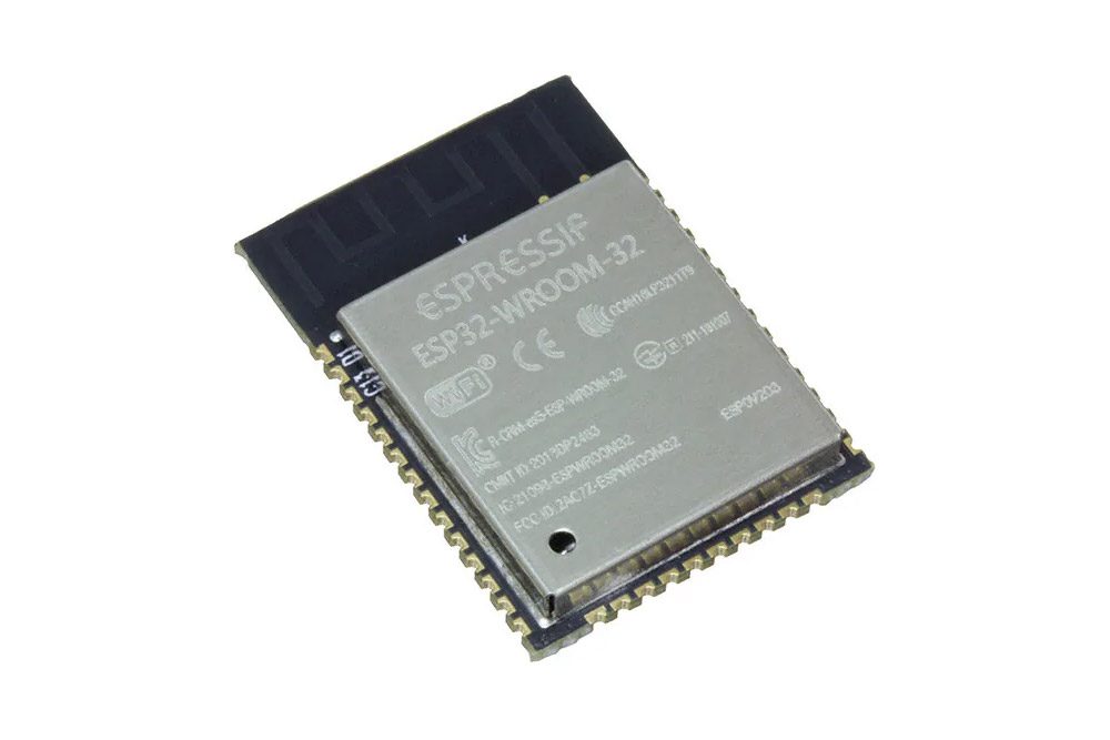
This ESP32-WROOM Wifi module uses castellated holes along the board edge to provide surface-mount connections to another board
Generally refers to any material used to create each layer in a PCB stackup.
Two forms of a PCB laminate material. The core refers to a laminate sheet with copper on both sides and the prepreg is used as a bonding layer.
Refers to a class of PCB laminate materials that have a Class 4 NEMA flammability rating. These are standard materials used to build PCBs.
A popular series of high frequency PCB laminate materials that are commonly used in RF/wireless systems.
Two types of layers in a PCB stackup. Plane layers have a complete layer of copper covering the entire laminate, while signal layers are etched with traces, polygons, and other copper features.
Two principal copper features on a printed circuit board. Traces connect the pads on component land patterns, while polygons are used to fill in the space between traces with copper to provide grounding and shielding. A trace is also called a track.
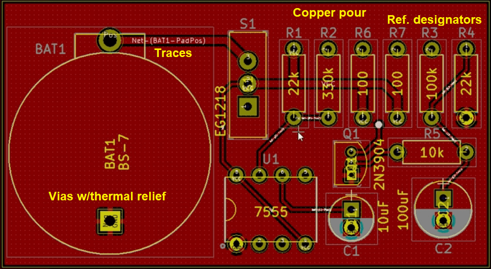
Copper pour, traces, vias, and reference designators in a KiCAD PCB layout.
A polygon is often called a polygon pour or copper pour. Filling in the empty space on a PCB with grounded copper provides shielding against EMI.
A controlled-depth drilling process used to remove via stubs from through-hole vias when a layer transition does not span the entire board thickness.
Used to fabricate microvias in a PCB.
A chemical process used to remove leftover drilling debris from holes in a PCB panel.
Leftover drilling debris on a PCB. This is often some leftover ridge of material attached to the wall of the drill hole.
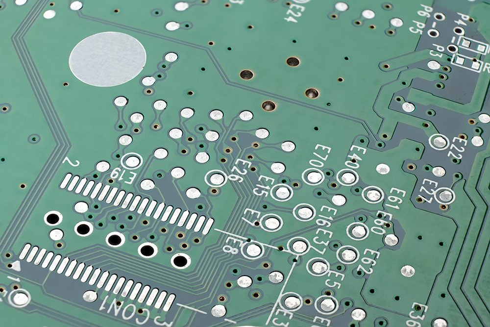
A process where copper is deposited from a plating solution via an electrochemical reaction. This is used to plate hole walls in plated through-hole vias, mounting holes, and other features on a PCB.
An alternative copper depositing process that uses a catalytic plating solution without an electrical current. This process can be used before electrodeposition or electroplating to apply a thin seed layer of copper prior to hole walls or other features. This process is also used when applying surface finishes to conductors (see below).
Another electrodeposition process that uses an electrochemical reaction for copper deposition.
CONDUCTOR SURFACE FINISH TERMINOLOGY
When a bare board is fabricated, the exposed conductors are normally plated with a surface finish to prevent problems with corrosion and to provide a solderable surface. The surface finish gives the conductors their particular luster and will be a major determinant of product reliability in specific applications.
A chemical bath process where a silver coating is applied to exposed copper on a PCB panel.
A water-based surface finish that selectively bonds to exposed copper to aid soldering. This is not recommended for use with through-hole components .
A process where exposed copper is plated with a solder alloy in a chemical bath process. This is sometimes called lead-free HASL when a lead-free solder alloy is used.
Surface plating processes give exposed conductors their shine and solderability
A thin gold surface plating applied over a nickel plating on all exposed conductors. Nickel is first plated onto copper, followed by gold plating. This is often used for fine pitch components and provides a strong solder joint.
An electrolytic deposition process where gold is plated over a nickel surface finish.
Similar to ENIG, but palladium is plated over nickel before applying gold plating. This process is used when corrosion is a major concern.
At Ultra Librarian, we care deeply about the success of all PCB designers and engineers, and we strive to provide resources to help new designers advance their careers. In addition to our glossary on PCB fabrication terminology, one of the resources we provide is a comprehensive electronics search engine that helps designers find the components they need. All Ultra Librarian users can access CAD models for components and verified 3D models that can be imported into popular ECAD applications. We also give users access to aggregated sourcing information from worldwide distributors.

Gold plating is often used for the teeth connectors on edge cards
Working with Ultra Librarian sets up your team for success to ensure streamlined and error-free design, production, and sourcing. Register today for free.