 A harsh environment is tough on electronics. Analog to digital conversion in a high temperature and highly electric/magnetic environment is always challenging. General sensors can barely produce reliable results.
Though radiation-hardened ICs appear reasonable, the focus is more on meeting the growing demands of modern communication systems. Texas Instruments’ integrated circuits and reference designs help you create communications payload systems complete with schematics, test data and design files.
Modern communications payload designs require:
- Wide bandwidth ADCs and DACs to provide the highest data throughput systems.
- Ultra-low jitter clocking solutions to maximize the performance of your data converters.
- Highly integrated, point-of-load (POL) solutions for the space market that reduce overall board size required for even the highest power processing boards.
Additionally, to maximize onboard decision-making, modern space-grade projects expect radiation-hardened ICs to have higher power densities, smaller footprints, and point-of-load (POL) solutions without compromising reliability and capability.
In this regard, TI’s ADC12DJ3200 is a 12-bit, dual-channel RF-Sampling high speed ADC with a buffered analog input that ticks all the boxes. The ADC12DJ3200 delivers the highest bandwidth (>7 GHz) in harsh radiation environments. This allows you to support multiple communication channels with higher throughput in a smaller amount of space. Additionally, it supports advanced radar imaging applications. With the highest data throughput and ultra-low jitter clocking solutions, ADC12DJ3200 features point-of-load (POL) solutions to meet space-grade power management application and requirements quickly.
What to Know About the ADC12DJ3200
TI’s ADC12DJ3200 is a 12-bit dual-channel ADC built for harsh environments with a wide input range and internal supply and reference capacitors. ADC12DJ3200 can sample up to 6400 Mega Samples per Second (MSPS) in a single channel mode (Nyquist bandwidth) and up to 34200 MSPS in a dual channel mode at 12-bit depth.
Thus, it not only offers a high channel count but also successfully avoids aliasing. It can directly sample input frequencies from DC to above 10GHz. This ADC gives you high speed and high resolution with ultra-low power conversion. Moreover, it can achieve unparalleled precision up to +150°C.
 Salient Features
- Low power, 12-bit, dual 3.2-GSPS/single 6.4-GSPS, RF-sampling ADC core
- Buffered analog input bandwidth (–3 dB): 7 GHz
- Usable input frequency range: >10 GHz
- Noiseless aperture delay (tAD) adjustment
- Automatic SYSREF timing calibration
- Total Ionizing Dose (TID): 300 krad (Si)
- Single Event Latchup (SEL): 120 MeV-cm2/mg
- Integrated digital down converter
- JESD204B subclass-1 compliant interface with up to 16 lanes
Typical Applications
Due to its high bandwidth of 8GHz, this high speed ADC is highly sought-after in many applications such as:
- Radars
- Satellite communications
- Oscilloscopes
- Software-defined Radios
- Communication testers
- Spectrometry
- Microwave backhaul
How the ADC12DJ3200 Meets Harsh Environment Requirements
JESD204B Interface
A high-speed JESD204B output lets the ADC interface with most hosts without requiring any external voltage shifter. The interface comes with Subclass 1 compliance to achieve deterministic latency using an external “SYSREF” as a timing signal.
Systems in harsh environments are sensitive to latency variation. Some examples of such systems are phased-array radars, beam-forming antennas, and medical imaging equipment. Thus, the deterministic link latency feature of ADC12DJ3200 enables systems requiring multi-device synchronization to achieve synchronization from startup to startup.
When multi-ADC synchronization and deterministic latency are not imperative, the device can also meet Subclass 0 compatibility. As a result, the device offers higher line rates up to 12.8 Gbps in the JESD204B standard while supporting up to 16 lanes alignment within a single device without external circuitry.
Advanced Synchronization
The ADC has advanced synchronization features. The clocking sub system has a noiseless aperture delay (tAD) adjustment, an SYSREF capture block, and a clock duty cycle corrector. Using tAD adjustment, you can shift the sampling instance of the ADC in exemplary steps to synchronize multiple ADCs, fine-tune system latency, or sample an ideal location of a frontend track and hold (T&H) amplifier output. Further, tAD adjust can be used for automatic SYSREF calibration to simplify synchronization.
SYSREF signal is essential for achieving repeatable system latencies and synchronization. However, in high speed ADCs, the higher device clock rate reduces the setup-and-hold window for SYSREF. The ADC12DJ3200 features automatic SYSREF timing calibration to measure invalid timing and choose an optimal sampling location with ease.
Optional Digital Down Converters (DDCs)
The ADC12DJ3200 offers DDC blocks in a dual-channel mode for frequency conversion and decimation. The sample can be decimated by overall decimation of 2, 4, 8, or 16 with a resolution of 15 bits. It helps to keep the ADC data rate reasonable for the data capture and to improve spectral performance.
Decimation is accompanied by filtering to reduce overall noise. Each DDC channel has four independent 32-Bit NCOs to produce alias-free complex output bandwidths of 80% of the effective output data rate. The best part is that this digital processing does not hamper the converter’s noise spectral density (NSD).
Radiation-Hardened
ADC12DJ3200QML-SP easily lets you move your space level design from COTs to Rad-Hard, sharing the same SoC architecture as in ADC12DJ3200. It is SEL (Single Event Latchup) immune with total ionizing dose performance of 300 krad without any functional interrupts. Higher SEU (Single Event Upset) rates are dealt with using latch up immune parts with linear energy transfer [LET] of 120 MeV/mg-cm2.
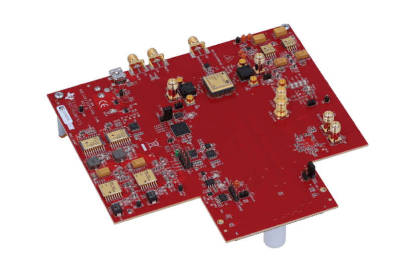
You can further take advantage of TI’s ADC12DJ3200EVMCVAL- an evaluation module (EVM)- to configure the ADC12DJ3200QML-SP device via flexible transformer-coupled analog inputs for a variety of sources and frequencies through a USB interface.
In order to best use the ADC12DJ3200 high speed ADC to your advantage, you need datasheet, footprints and CAD/ECAD layouts at one place. In this regard, Ultra Librarian offers a comprehensive online resource to fetch all these details with a single click.
Working with Ultra Librarian sets up your team for success to ensure streamlined and error-free design, production, and sourcing. Register today for free.