ADS1299 ADC
Arguably, the most significant advances in medical treatment have been achieved due to advanced electronics. Specifically, the ability to capture and analyze biological data electronically that can be scientifically evaluated using computational algorithms and displayed in digestible formats like graphs is invaluable in performing root-cause analysis of some of the most challenging medical conditions. A core component of the electronic systems that perform these studies is the analog to digital converter. One of the most implemented of these devices is described in detail in the ADS1299 datasheet.
ADS1299: Features and Applications
The design of medical device PCBs requires the understanding and observance of many important standards and best practices. Obviously, the primary concern for any device that is invasive or interacts with the human body demands special attention to safety. It is also important that such devices are able to capture and process low-level signals with minimal interference or noise propagation. The ADS1299 analog to digital converter (ADC) exhibits these essential characteristics, which makes this device a favorite for medical instrumentation products.
As presented in the ADS1299 datasheet, the converter has several attractive features that can be leveraged for medical equipment applications.
*SPS denotes samples per second.
The features above are specifically beneficial for the common applications of the ADS1299.
Common Applications
- Fetal ECG monitoring
- EEG study
- Bispectral Index (BIS)
- Evoked Audio Potential (EAP)
- Sleep Study monitoring
As listed above, the ADS1299 is a low noise multichannel converter with flexible programmable gain and low current biasing requirements. The device comes in 4, 6, or 8 channel configurations, each with simultaneous sampling capability, internal reference and oscillator, and 24-bit operation. When designing medical circuit boards or electronic systems using the ADS1299, it is important to fully understand its specifications and characteristics.
ADS1299: Specifications and Characteristics
The constraints on voltages, current, and temperature for the ADS1299 are listed in the table below.
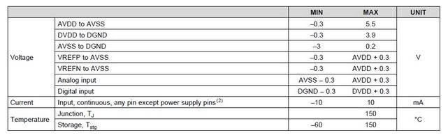
Absolute maximum ratings for ADS1299
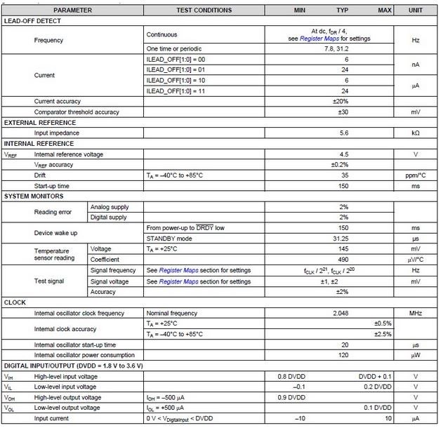
As shown above, the ADS1299 has both analog and digital power supplies and accepts both signal types. The electrical parameters for the ASC are shown in the tables below.
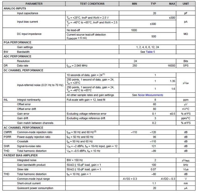
ADS1299 electrical characteristics (a)
ADS1299 electrical characteristics (b)
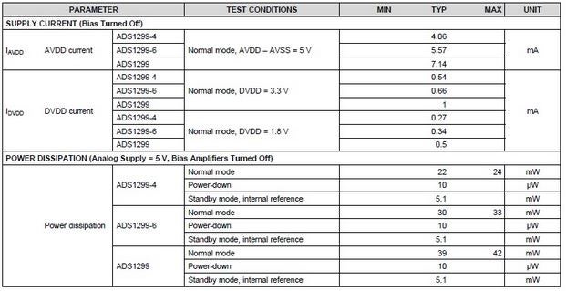
ADS1299 electrical characteristics (c)
It is notable that the ADS1299 has low power dissipation ratings for all three operation modes: Normal, Power-down, and Standby. In addition to electrical and thermal characteristics, effective design requires knowing the device’s PCB layout and operation.
ADS1299: Architecture and Operation
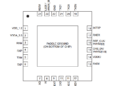
The ADS1299–for 4, 6, and 8 channels–comes in a 64-pin TQFP, which is a standard IC package format.
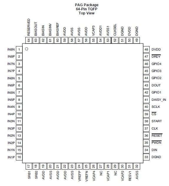
ADS1299 pinout
The device pin descriptions, shown below, are described fully in the ADS1299 datasheet.
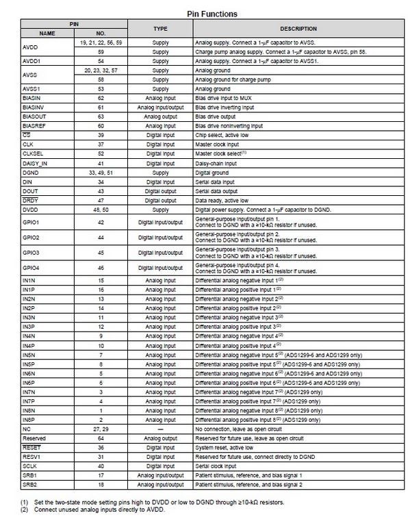
Pin descriptions for the ADS1299
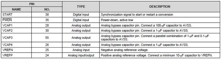
Additional pin descriptions for the ADS1299
The device has several control pins, as presented above. These can be understood best by reviewing the functional diagram below.
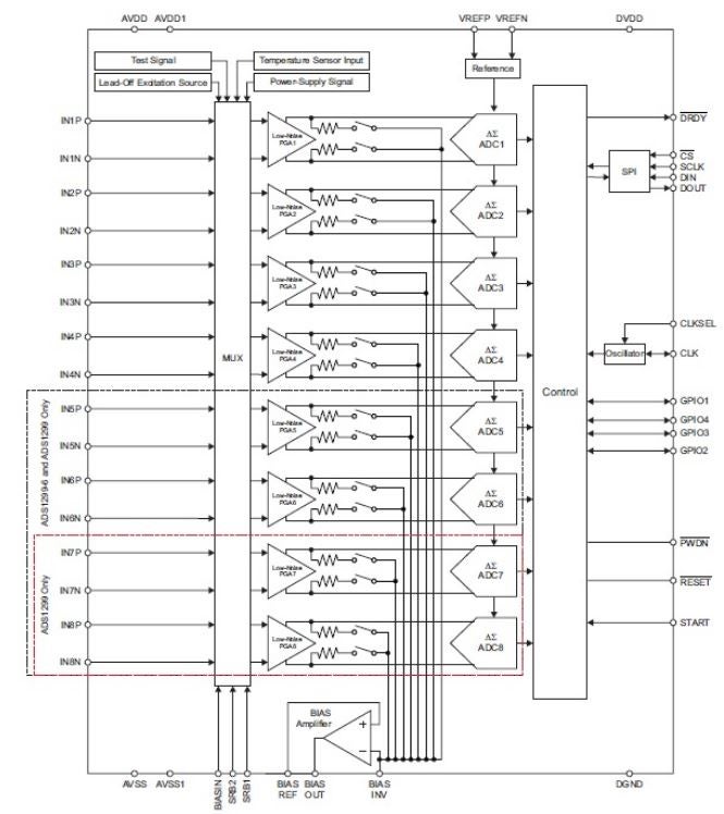
Functional diagram of the ADS1299
The ADC includes a series of multiplexers, as shown above. These switches can be configured in a wide array of configurations and add to the converters flexibility. Both a differential and pseudo-differential input can be used to drive the device. For linear operation, it is important to keep the inputs (and gain) such that the outputs do not get too close to the supply voltages, AVSS and AVDD. The ADS1299 does require a number of external passive components to control functionality, help minimize noise, and ensure reliable operation.
PCB Development with the ADS1299 Datasheet
The ADS1299 datasheet provides a wealth of information to assist you in designing your medical PCB. This includes an example layout that can be used as a basis for your implementation with the ADS1299.
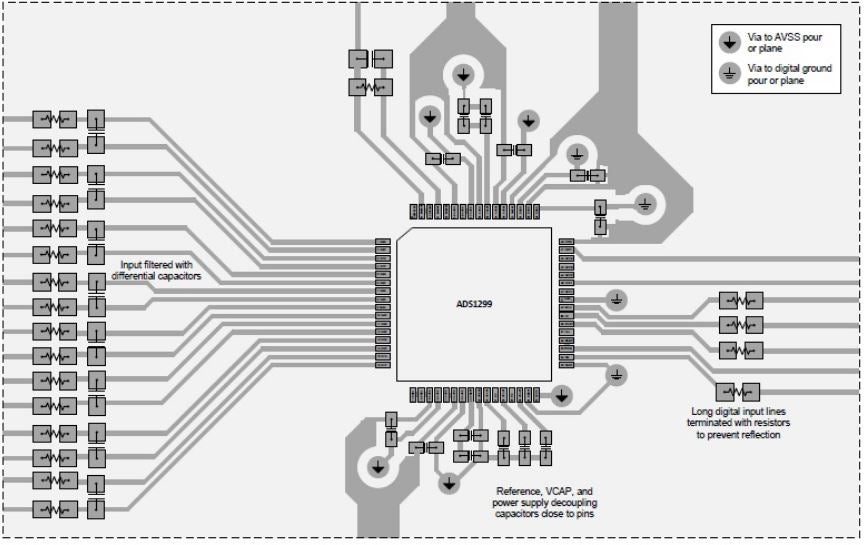
PCB layout example of the ADS1299
As shown, there can be significant fanout with the ADS1299. However, the device itself comes in a 12.2 x 12.2 mm2 quad flat pack. In addition to electrical characteristics, constraints, and physical dimensions for your PCB layout design, the datasheet also includes programming information; including a flowchart of the startup algorithm to prepare the converter for medical data capture, shown below.
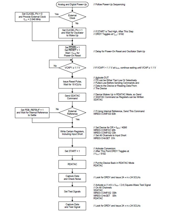
ADS1299 sample setup flowchart
The ADS1299 is a great choice for your medical PCB design. However, it is important to utilize the ADS1299 datasheet to ensure that you incorporate requirements, adhere to constraints, and take advantage of the converter’s advantages and benefits.
If you’re looking for CAD models for common components or important information like how to best use the ADS1299 datasheet for your design, Ultra Librarian helps by compiling all your sourcing and CAD information in one place.
Working with Ultra Librarian sets up your team for success to ensure streamlined and error-free design, production, and sourcing. Register today for free.